MLD1N06CLT4G ON Semiconductor, MLD1N06CLT4G Datasheet
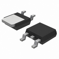
IC MOSFET POWER N-CH 1A 62V DPAK

MLD1N06CLT4G

Manufacturer Part Number
MLD1N06CLT4G
Description
IC MOSFET POWER N-CH 1A 62V DPAK
Manufacturer
ON Semiconductor
Series
SMARTDISCRETES™r
Datasheet

Specifications of MLD1N06CLT4G

Transistor Type
NPN, N-Channel Gate-Drain, Source Clamp
Voltage - Rated
62V
Current Rating
1A
Mounting Type
Surface Mount
Package / Case
TO-252-3, DPak (2 Leads + Tab), SC-63
Lead Free Status / RoHS Status
Lead free / RoHS Compliant
Other names
MLD1N06CLT4GOS
MLD1N06CLT4GOS
MLD1N06CLT4GOSTR

Available stocks

Company
Part Number
Manufacturer
Quantity
Price
Part Number:
MLD1N06CLT4G
Manufacturer:
ATMEL
Quantity:
1 000
Part Number:
MLD1N06CLT4G
Manufacturer:
ON
Quantity:
12 500
Part Number:
MLD1N06CLT4G
Manufacturer:
ON
Quantity:
12 500
MLD1N06CL
SMARTDISCRETESt MOSFET
1 Amp, 62 Volts, Logic Level
N−Channel DPAK
power switching device with short circuit protection that can be
directly interfaced to a microcontrol unit (MCU). Ideal applications
include automotive fuel injector driver, incandescent lamp driver or
other applications where a high in−rush current or a shorted load
condition could occur.
short circuit protection, integrated Gate−Source clamping for ESD
protection and integral Gate−Drain clamping for over−voltage
protection and Sensefet technology for low on−resistance. No
additional gate series resistance is required when interfacing to the
output of a MCU, but a 40 kW gate pulldown resistor is recommended
to avoid a floating gate condition.
to be applied without use of external transient suppression
components. The Gate−Source clamp protects the MOSFET input
from electrostatic voltage stress up to 2.0 kV. The Gate−Drain clamp
protects the MOSFET drain from the avalanche stress that occurs with
inductive loads. Their unique design provides voltage clamping that is
essentially independent of operating temperature.
Features
Stresses exceeding Maximum Ratings may damage the device. Maximum
Ratings are stress ratings only. Functional operation above the Recommended
Operating Conditions is not implied. Extended exposure to stresses above the
Recommended Operating Conditions may affect device reliability.
1. When surface mounted to an FR−4 board using the minimum recommended
2. When surface mounted to an FR−4 board using the 0.5 sq.in. drain pad size.
© Semiconductor Components Industries, LLC, 2008
September, 2008 − Rev. 4
MAXIMUM RATINGS
THERMAL CHARACTERISTICS
Drain−to−Source Voltage
Drain−to−Gate Voltage (R
Gate−to−Source Voltage
Drain Current
Total Power Dissipation
Operating and Storage Temperature Range
Electrostatic Discharge Voltage
Thermal Resistance
Maximum Lead Temperature for Soldering
Purposes, 1/8″ from case for 5 seconds
The MLD1N06CL is designed for applications that require a rugged
This Logic Level Power MOSFET features current limiting for
The internal Gate−Source and Gate−Drain clamps allow the device
Pb−Free Package is Available
pad size.
(Human Model)
Junction−to−Case
Junction−to−Ambient (Note 1)
Junction−to−Ambient (Note 2)
− Continuous
− Continuous
− Single Pulse
Rating
(T
GS
J
= 25°C unless otherwise noted)
= 1.0 MW)
Preferred Device
Symbol
T
V
V
R
R
R
J
ESD
V
I
P
DGR
, T
T
DSS
DM
I
qJC
qJA
qJA
GS
D
D
L
stg
Self−limited
−50 to 150
Clamped
Clamped
Value
3.12
71.4
±10
100
260
1.8
2.0
40
1
°C/W
Unit
Vdc
Vdc
Vdc
Adc
Apk
°C
kV
°C
W
†For information on tape and reel specifications,
Preferred devices are recommended choices for future use
and best overall value.
MLD1N06CLT4
MLD1N06CLT4G
62 V (Clamped)
including part orientation and tape sizes, please
refer to our Tape and Reel Packaging Specification
Brochure, BRD8011/D.
1 2
V
Device
(BR)DSS
3
ORDERING INFORMATION
G
Y
WW
L1N06C
G
4
http://onsemi.com
CASE 369C
STYLE 2
(Pb−Free)
Package
N−Channel
R
R1
DPAK
DPAK
DPAK
DS(on)
750 mW
= Year
= Work Week
= Device Code
= Pb−Free Package
Publication Order Number:
TYP
R2
2500 Tape & Reel
2500 Tape & Reel
MARKING
DIAGRAM
D
S
MLD1N06CL/D
Shipping
06CG
YWW
I
D
L1N
1.0 A
MAX

Related parts for MLD1N06CLT4G

MLD1N06CLT4G Summary of contents

Page 1

... ESD 2.0 kV °C/W MLD1N06CLT4 R 3.12 qJC R 100 qJA MLD1N06CLT4G 71.4 R qJA T 260 °C L †For information on tape and reel specifications, including part orientation and tape sizes, please refer to our Tape and Reel Packaging Specification Brochure, BRD8011/D. Preferred devices are recommended choices for future use and best overall value ...

Page 2

UNCLAMPED DRAIN−TO−SOURCE AVALANCHE CHARACTERISTICS Rating Single Pulse Drain−to−Source Avalanche Energy Starting T ELECTRICAL CHARACTERISTICS Characteristic OFF CHARACTERISTICS Drain−to−Source Breakdown Voltage (Internally Clamped mAdc Vdc mAdc Vdc, ...

Page 3

V , DRAIN-TO-SOURCE VOLTAGE (VOLTS) DS Figure 1. Output Characteristics THE SMARTDISCRETES CONCEPT From a standard power MOSFET process, several active and passive elements can be obtained that provide on−chip protection to ...

Page 4

T , JUNCTION TEMPERATURE (°C) J Figure 3. I Variation D(lim) With Temperature 1.25 1 0.75 0.5 0.25 -50 100 100 T , JUNCTION ...

Page 5

... The curves are based on a case temperature of 25°C and a maximum junction temperature of 150°C. Limitations for repetitive pulses at various case temperatures can be determined by using the thermal response curves. ON Semiconductor Application Note, AN569, “Transient Thermal Resistance − General Data and Its Use” provides detailed instructions. MAXIMUM DC VOLTAGE CONSIDERATIONS The maximum drain− ...

Page 6

V PULSE GENERATOR gen 50W Figure 10. Switching Test Circuit ACTIVE CLAMPING SMARTDISCRETES technology can provide on−chip realization of the popular gate−to−source and gate−to−drain Zener diode clamp elements. Until recently, such features have been implemented ...

Page 7

... PL G 0.13 (0.005) *For additional information on our Pb−Free strategy and soldering details, please download the ON Semiconductor Soldering and Mounting Techniques Reference Manual, SOLDERRM/D. SMARTDISCRETES is a trademark of Semiconductor Components Industries, LLC (SCILLC). ON Semiconductor and are registered trademarks of Semiconductor Components Industries, LLC (SCILLC). SCILLC reserves the right to make changes without further notice to any products herein ...

Related keywords