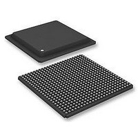
XC6SLX150T-2FGG484C Xilinx Inc, XC6SLX150T-2FGG484C Datasheet - Page 4

XC6SLX150T-2FGG484C
Manufacturer Part Number
XC6SLX150T-2FGG484C
Description
FPGA, SPARTAN-6 LXT, 147K, 484FGGBGA
Manufacturer
Xilinx Inc
Series
Spartan® 6 LXTr
Specifications of XC6SLX150T-2FGG484C
No. Of Logic Blocks
23038
No. Of Macrocells
147443
Family Type
Spartan-6
No. Of Speed Grades
2
Total Ram Bits
4939776
No. Of I/o's
296
Clock Management
DCM, PLL
I/o Supply Voltage
3.3V
Number Of Logic Elements/cells
147443
Number Of Labs/clbs
11519
Number Of I /o
296
Voltage - Supply
1.14 V ~ 1.26 V
Mounting Type
Surface Mount
Operating Temperature
0°C ~ 85°C
Package / Case
484-BBGA
Rohs Compliant
Yes
Lead Free Status / RoHS Status
Lead free / RoHS Compliant
Number Of Gates
-
Lead Free Status / RoHS Status
Lead free / RoHS Compliant, Lead free / RoHS Compliant
Available stocks
Company
Part Number
Manufacturer
Quantity
Price
Company:
Part Number:
XC6SLX150T-2FGG484C
Manufacturer:
Xilinx Inc
Quantity:
10 000
Table 4: DC Characteristics Over Recommended Operating Conditions
DS162 (v2.0) March 31, 2011
Preliminary Product Specification
Notes:
1.
2.
3.
4.
R
Symbol
IN_TERM
V
I
V
R
BATT
DRAUX
Maximum value specified for worst case process at 25°C. XC6SLX75, XC6SLX75T, XC6SLX100, XC6SLX100T, XC6SLX150, and XC6SLX150T
only.
Refer to IBIS models for R
V
Termination resistance to a V
I
I
DRINT
I
C
I
RPU
RPD
REF
DT
HS
CCO2
I
L
IN
(2)
(1)
(4)
is not required for data retention. The minimum V
Data retention V
Data retention V
V
Input or output leakage current per pin (sample-tested)
Leakage current on pins during hot
socketing with FPGA unpowered
Die input capacitance at the pad
Pad pull-up (when selected) @ V
Pad pull-up (when selected) @ V
Pad pull-up (when selected) @ V
Pad pull-up (when selected) @ V
Pad pull-up (when selected) @ V
Pad pull-down (when selected) @ V
Pad pull-down (when selected) @ V
Battery supply current
Resistance of optional input differential termination circuit, V
Thevenin equivalent resistance of programmable input termination
(UNTUNED_SPLIT_25)
Thevenin equivalent resistance of programmable input termination
(UNTUNED_SPLIT_50)
Thevenin equivalent resistance of programmable input termination
(UNTUNED_SPLIT_75)
REF
leakage current per pin
DT
CCO
variation and for values at V
CCINT
CCAUX
/2 level.
voltage (below which configuration data might be lost)
voltage (below which configuration data might be lost)
IN
IN
IN
IN
IN
= 0V, V
= 0V, V
= 0V, V
= 0V, V
= 0V, V
IN
IN
Description
= V
= V
CCO2
CCAUX
All pins except PROGRAM_B, DONE, and
JTAG pins when HSWAPEN = 1
PROGRAM_B, DONE, and JTAG pins, or other
pins when HSWAPEN = 0
CCO
CCO
CCO
CCO
CCO
CCO
CCO
for power-on reset and configuration is 1.65V.
www.xilinx.com
Spartan-6 FPGA Data Sheet: DC and Switching Characteristics
, V
, V
= 2.5V. IBIS values for R
= 3.3V or V
= 2.5V or V
= 1.8V
= 1.5V
= 1.2V
CCAUX
CCAUX
= 3.3V
= 2.5V
CCAUX
CCAUX
CCAUX
= 3.3V
= 2.5V
= 3.3V
DT
are valid for all temperature ranges.
Min
–10
–10
–20
200
140
200
120
0.8
2.0
60
40
12
23
39
56
–
–
–
I
HS
Typ
100
+ I
25
50
75
–
–
–
–
–
–
–
–
–
–
–
–
–
–
RPU
Max
500
350
200
150
100
550
400
150
109
10
10
20
10
55
72
–
–
–
Units
µA
µA
µA
µA
pF
µA
µA
µA
µA
µA
µA
µA
nA
V
V
4


