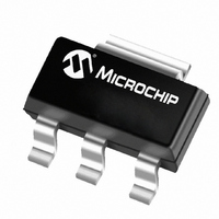
MCP1826ST-0802E/DB Microchip Technology, MCP1826ST-0802E/DB Datasheet - Page 19

MCP1826ST-0802E/DB
Manufacturer Part Number
MCP1826ST-0802E/DB
Description
1A CMOS LDO, Vout=0.8V, Extended Temp Range 3 SOT-223 T/R
Manufacturer
Microchip Technology
Datasheet
1.MCP1826T-1202EDC.pdf
(36 pages)
Specifications of MCP1826ST-0802E/DB
Regulator Topology
Positive Fixed
Voltage - Output
0.8V
Voltage - Input
2.3 ~ 6 V
Voltage - Dropout (typical)
0.25V @ 1A
Number Of Regulators
1
Current - Output
1A (Min)
Operating Temperature
-40°C ~ 125°C
Mounting Type
Surface Mount
Package / Case
SOT-223 (3 leads + Tab), SC-73, TO-261
Lead Free Status / RoHS Status
Lead free / RoHS Compliant
Current - Limit (min)
-
Lead Free Status / RoHS Status
Lead free / RoHS Compliant
Other names
MCP1826ST-0802E/DBTR
5.0
5.1
The MCP1826/MCP1826S is used for applications that
require high LDO output current and a power good
output.
FIGURE 5-1:
5.1.1
5.2
5.2.1
The internal power dissipation within the MCP1826/
MCP1826S is a function of input voltage, output
voltage,
Equation 5-1 can be used to calculate the internal
power dissipation for the LDO.
EQUATION 5-1:
© 2007 Microchip Technology Inc.
Off
3.3V
Input Voltage Range = 3.3V ± 5%
Where:
P
On
Temperature Rise = 28.27
V
LDO
V
V
OUT(MIN)
Package Type = TO-220-5
P
DROPOUT (max)
IN(MAX)
V
V
APPLICATION CIRCUITS/
ISSUES
Typical Application
V
Power Calculations
DISS
OUT
P
SHDN
IN
output
=
IN
V
LDO
APPLICATION CONDITIONS
POWER DISSIPATION
IN
4.7 µF
C
maximum = 3.465V
(
minimum = 3.135V
1
V
(typical) = 2.5V
(typical) = 0.965W
IN MAX )
(
= LDO Pass device internal
= Maximum input voltage
= LDO minimum output voltage
MCP1826-2.5
1
I
OUT
current
2
power dissipation
3 4 5
Typical Application Circuit.
= 0.350V
= 1000 mA maximum
)
GND
–
V
OUT MIN
and
(
°
C
V
10 kΩ
OUT
quiescent
)
) I
R
×
1
= 2.5V @ 1000 mA
OUT MAX )
PWRGD
(
C
10 µF
current.
2
)
MCP1826/MCP1826S
In addition to the LDO pass element power dissipation,
there is power dissipation within the MCP1826/
MCP1826S as a result of quiescent or ground current.
The power dissipation as a result of the ground current
can be calculated using the following equation:
EQUATION 5-2:
The total power dissipated within the MCP1826/
MCP1826S is the sum of the power dissipated in the
LDO pass device and the P(I
CMOS construction, the typical I
MCP1826S is 120 µA. Operating at a maximum V
3.465V results in a power dissipation of 0.12 milli-Watts
for a 2.5V output. For most applications, this is small
compared to the LDO pass device power dissipation
and can be neglected.
The
temperature specified for the MCP1826/MCP1826S is
+125
of the MCP1826/MCP1826S, the total internal power
dissipation is multiplied by the thermal resistance from
junction to ambient (Rθ
resistance from junction to ambient for the TO-220-5
package is estimated at 29.3
EQUATION 5-3:
Where:
T
P
°
T
J(MAX)
C
TOTAL
V
AMAX
Rθ
maximum
.
IN(MAX)
P
To estimate the internal junction temperature
JA
T
I(GND
J MAX
I
VIN
(
= Maximum continuous junction
= Total device power dissipation
= Thermal resistance from junction to
= Maximum ambient temperature
P
I GND
temperature
ambient
(
)
= Power dissipation due to the
= Maximum input voltage
= Current flowing in the V
=
continuous
)
P
quiescent current of the LDO
with no LDO output current
(LDO quiescent current)
TOTAL
=
JA
V
) of the device. The thermal
IN MAX
GND
(
°
×
C/W.
Rθ
GND
) term. Because of the
)
JA
operating
×
+
I
DS22057A-page 19
for the MCP1826/
VIN
T
AMAX
IN
junction
pin
IN
of


