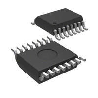
MIC2583-MBQS Micrel Inc, MIC2583-MBQS Datasheet - Page 17

MIC2583-MBQS
Manufacturer Part Number
MIC2583-MBQS
Description
IC,Power Control/Management,CMOS,SSOP,16PIN,PLASTIC
Manufacturer
Micrel Inc
Type
Hot-Swap Controllerr
Datasheet
1.MIC2582-JYM.pdf
(25 pages)
Specifications of MIC2583-MBQS
Applications
General Purpose
Internal Switch(s)
No
Voltage - Supply
2.3 V ~ 13.2 V
Operating Temperature
-40°C ~ 85°C
Mounting Type
Surface Mount
Package / Case
16-SSOP (0.150", 3.90mm Width)
Linear Misc Type
Positive Low Voltage
Family Name
MIC2583
Package Type
QSOP
Operating Supply Voltage (min)
2.3V
Operating Supply Voltage (max)
13.2V
Operating Temperature (min)
-40C
Operating Temperature (max)
85C
Operating Temperature Classification
Industrial
Product Depth (mm)
3.99mm
Product Height (mm)
1.4mm
Product Length (mm)
4.98mm
Mounting
Surface Mount
Pin Count
16
Lead Free Status / RoHS Status
Contains lead / RoHS non-compliant
Lead Free Status / RoHS Status
Contains lead / RoHS non-compliant
12V in this example, and the ON pin voltage exceeds its
threshold (VON) of 1.24V and the MIC2582/83 initiates a
start-up cycle. In Figure 6, the connection sense consisting
of a discrete logic-level MOSFET and a few resistors allows
for interrupt control from the processor or other signal
controller to shut off the output of the MIC2582/83. R4 pulls
the GATE of Q2 to V
connectors are fully mated.
Once the connectors fully mate, a logic LOW at the
/ON_OFF signal turns Q2 off and allows the ON pin to pull
up above its threshold and initiate a start-up cycle. Applying
a logic HIGH at the /ON_OFF signal will turn Q2 on and
short the ON pin of the MIC2582/83 to ground which turns
off the GATE output charge pump.
Higher UVLO Setting
Once a PCB is inserted into a backplane (power supply), the
internal UVLO circuit of the MIC2582/83 holds the GATE
output charge pump off until VCC exceeds 2.2V. If VCC falls
below 2.1V, the UVLO circuit pulls the GATE output to
ground and clears the overvoltage and/or current limit faults.
A typical 12V application, for example, should implement a
higher UVLO than the internal 2.1V threshold of MIC2582 to
avoid delivering power to downstream modules/loads while
the input is below tolerance. For a higher UVLO threshold,
the circuit in Figure 7 can be used to delay the output
MOSFET from switching on until the desired input voltage is
achieved. The circuit allows the charge pump to remain off
until V
will be shut down when V
the example circuit (Figure 7), the rising UVLO threshold is
set at approximately 9.5V and the falling UVLO threshold is
established as 9.1V. The circuit consists of an external
resistor divider at the ON pin that keeps the GATE output
charge pump off until the voltage at the ON pin exceeds its
threshold (V
Micrel, Inc.
April 2009
IN
exceeds
ON
) and after the start-up timer elapses.
⎛
⎜
⎝
1
+
IN
R
R
and the ON pin is held low until the
2
1
IN
⎞
⎟
⎠
×
falls below
. 1
24
V
.
The GATE drive output
⎛
⎜
⎝
1
+
R
R
2
1
⎞
⎟
⎠
×
Figure 7. Higher UVLO Setting
. 1
19
V
.
In
17
5V Switch with 3.3V Supply Generation
The MIC2582/83 can be configured to switch a primary
supply while generating a secondary regulated voltage rail.
The circuit in Figure 8 enables the MIC2582 to switch a 5V
supply while also providing a 3.3V low dropout regulated
supply with only a few added external components. Upon
enabling the MIC2582, the GATE output voltage increases
and thus the 3.3V supply also begins to ramp. As the 3.3V
output supply crosses 3.3V, the FB pin threshold is also
exceeded which triggers the power-on reset comparator.
The /POR pin goes HIGH, turning on transistor Q3 which
lowers the voltage on the gate of MOSFET Q2. The result is
a regulated 3.3V supply with the gate feedback loop of Q2
compensated by capacitor C3 and resistors R4 and R5. For
MOSFET Q2, special consideration must be given to the
power dissipation capability of the selected MOSFET as
1.5V to 2V will drop across the device during normal
operation in this application. Therefore, the device is
susceptible to overheating dependent upon the current
requirements for the regulated output. In this example, the
power dissipated by Q2 is approximately = 1W. However, a
substantial amount of power will be generated with higher
current requirements and/or conditions. As a general
guideline, expect the ambient temperature within the power
supply box to exceed the maximum operating ambient
temperature of the system environment by approximately
20ºC. Given the MOSFET’s R
dissipated by the MOSFET, an approximation for the
junction temperature at which the device will operate is
obtained as follows:
where T
implementation of additional copper heat sinking is highly
recommended for the area under/around the MOSFET.
T
J
= (P
A
D
= T
x R
θ(JA)
A (MAX OPERATING)
) + T
A
+ 20ºC. As a precaution, the
θ
(JA)
and the expected power
MIC2582/MIC2583
M9999-043009-C
(10)


