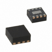
MIC5310-MGYML TR Micrel Inc, MIC5310-MGYML TR Datasheet - Page 8

MIC5310-MGYML TR
Manufacturer Part Number
MIC5310-MGYML TR
Description
Dual 150mA LDO In 2mm By 2mm MLFr ( Compliant)
Manufacturer
Micrel Inc
Datasheet
1.MIC5310-PGYML_TR.pdf
(10 pages)
Specifications of MIC5310-MGYML TR
Regulator Topology
Positive Fixed
Voltage - Output
2.8V, 1.8V
Voltage - Input
2.3 ~ 5.5 V
Voltage - Dropout (typical)
0.035V @ 150mA
Number Of Regulators
2
Current - Output
150mA
Current - Limit (min)
300mA
Operating Temperature
-40°C ~ 125°C
Mounting Type
Surface Mount
Package / Case
8-MLF®, QFN
Lead Free Status / RoHS Status
Lead free / RoHS Compliant
Other names
576-1566-2
August 2007
Applications Information
Enable/Shutdown
The MIC5310 comes with dual active-high enable pins
that allow each regulator to be enabled independently.
Forcing the enable pin low disables the regulator and
sends it into a “zero” off-mode-current state. In this
state, current consumed by the regulator goes nearly
to zero. Forcing the enable pin high enables the
output voltage. The active-high enable pin uses
CMOS technology and the enable pin cannot be left
floating; a floating enable pin may cause an
indeterminate state on the output.
Input Capacitor
The MIC5310 is a high-performance, high bandwidth
device. Therefore, it requires a well-bypassed input
supply for optimal performance. A 1µF capacitor is
required from the input to ground to provide stability.
Low-ESR
performance at a minimum of space. Additional high-
frequency capacitors, such as small-valued NPO
dielectric-type
frequency noise and are good practice in any RF-
based circuit.
Output Capacitor
The MIC5310 requires an output capacitor of 1µF or
greater to maintain stability. The design is optimized
for use with low-ESR ceramic chip capacitors. High
ESR capacitors may cause high frequency oscillation.
The
performance has been optimized for a 1µF ceramic
output capacitor and does not improve significantly
with larger capacitance.
X7R/X5R
recommended
performance.
capacitance by 15% over their operating temperature
range and are the most stable type of ceramic
capacitors. Z5U and Y5V dielectric capacitors change
value by as much as 50% and 60%, respectively, over
their operating temperature ranges. To use a ceramic
chip capacitor with Y5V dielectric, the value must be
much higher than an X7R ceramic capacitor to ensure
the same minimum capacitance over the equivalent
operating temperature range.
output
dielectric-type
ceramic
capacitor
capacitors,
because
X7R-type
capacitors
can
ceramic
of
help
capacitors
be
their
provide
filter
increased,
capacitors
temperature
out
change
optimal
high-
are
but
8
Bypass Capacitor
A capacitor can be placed from the noise bypass pin-
to-ground to reduce output voltage noise. The
capacitor bypasses the internal reference. A 0.1µF
capacitor is recommended for applications that require
low-noise outputs. The bypass capacitor can be
increased, further reducing noise and improving
PSRR. Turn-on time increases slightly with respect to
bypass capacitance. A unique, quick-start circuit
allows the MIC5310 to drive a large capacitor on the
bypass pin without significantly slowing turn-on time.
No-Load Stability
Unlike many other voltage regulators, the MIC5310
will remain stable and in regulation with no load. This
is especially important in CMOS RAM keep-alive
applications.
Thermal Considerations
The MIC5310 is designed to provide 150mA of
continuous current for both outputs in a very small
package. Maximum ambient operating temperature
can be calculated based on the output current and the
voltage drop across the part. Given that the input
voltage is 3.3V, the output voltage is 2.8V for V
1.5V for V
actual power dissipation of the regulator circuit can be
determined using the equation:
P
Because this device is CMOS and the ground current
is typically <100µA over the load range, the power
dissipation contributed by the ground current is < 1%
and can be ignored for this calculation.
P
To determine the maximum ambient operating
temperature of the package, use the junction-to-
ambient thermal resistance of the device and the
following basic equation:
T
the die θ
The table below shows junction-to-ambient thermal
resistance for the MIC5310 in different packages.
J(max)
D
D
= (V
= (3.3V – 2.8V) × 150mA + (3.3V -1.5) × 150mA
= 125°C, the maximum junction temperature of
IN
P
P
JA
– V
D
D(MAX)
OUT2
thermal resistance = 90°C/W.
= 0.345W
OUT1
and the output current = 150mA. The
=
) I
OUT1
⎝
⎛
T
+ (V
J(MAX)
IN
JA
– V
- T
OUT2
A
) I
M9999-082407-B
OUT2
+ V
IN
I
GND
OUT1
,


