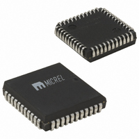
MM5450YV TR Micrel Inc, MM5450YV TR Datasheet - Page 5

MM5450YV TR
Manufacturer Part Number
MM5450YV TR
Description
LED Display Driver -
Manufacturer
Micrel Inc
Datasheet
1.MM5451YV_TR.pdf
(9 pages)
Specifications of MM5450YV TR
Display Type
LED
Interface
Serial
Current - Supply
10mA
Voltage - Supply
4.75 V ~ 11 V
Operating Temperature
-40°C ~ 85°C
Mounting Type
Surface Mount
Package / Case
44-LCC (J-Lead)
Operating Supply Voltage (typ)
5/9V
Number Of Digits
5
Operating Temperature (min)
-40C
Operating Temperature (max)
85C
Operating Temperature Classification
Industrial
Package Type
PLCC
Pin Count
44
Mounting
Surface Mount
Power Dissipation
1W
Operating Supply Voltage (min)
4.75V
Operating Supply Voltage (max)
11V
Lead Free Status / RoHS Status
Lead free / RoHS Compliant
Configuration
-
Digits Or Characters
-
Lead Free Status / Rohs Status
Compliant
Other names
576-1342-2
Functional Description
The MM5450 and MM5451 were designed to drive either
4- or 5-digit alphanumeric LED displays with the added
benefit of requiring minimal interface with the display or
data source.
Data is transferred serially via 2 signals; clock and serial
data. Data transfer without the added inconvenience of
an external load signal is accomplished by using a
format of a leading “1”followed by the allowed 35 data
bits. These 35 data bits are latched after the 36th has
been transferred. This scheme provides non multiplexed,
direct drive to the LED display. Characters currently
displayed (thus, data output) changes only if the serial
data bits differ from those previously transferred.
The MIC37252 regulator is fully protected from damage
due to fault conditions. Current limiting is provided. This
limiting is linear; output current during overload
conditions is constant. Thermal shutdown disables the
device when the die temperature exceeds the maximum
safe operating temperature. Transient protection allows
device (and load) survival even when the input voltage
spikes above and below nominal. The output structure of
these regulators allows voltages in excess of the desired
output voltage to be applied without reverse current flow.
Control of the output current for LED displays provides
for the display brightness. To prevent oscillations, a 1nF
capacitor should be connected to pin 19, brightness
control.
The block diagram is shown in Figure 1. For the
MIC5450, the /DATA ENABLE is a metal option and is
used instead of the 35th output. The output current is
typically 20-times greater that the current into pin 19,
which is set by an external variable resistor.
There is an external reset connection shown which is
available on unpackaged (die) only. Figure 2 illustrates
the die pad locations for bonding in “chip on board”
applications.
Micrel, Inc.
February 2006
5
Figure 5 shows the input data format. A leading “1” is
followed by 35 bits of data. After the 36th had been
transferred, a LOAD signal is generated synchronously
with the clock high state. This loads the 35 bits of data
into the latches. The low side of the clock is used to
generate a RESET signal which clears all shift registers
for the next set of data. All shift registers are static
master-slave, with no clear for the master portion of the
first register, allowing continuous operation.
There must be a complete set of 36 clocks or the shift
registers will not clear.
When the chip first powers ON, an internal power ON
reset signal is generated which resets all registers and
all latches. The START bit and the first clock return the
chip to its normal operation.
Figure 3 and 4 show the pinout of the MIC5450 and
MIC5451. Bit 1 is the first bit following the start bit and it
will appear on pin 18. A logical “1” at the input will turn
on the appropriate LED.
Figure 5 shows the timing relationships between data,
clock and /DATA ENABLE. A maximum clock frequency
of 0.5MHz is assumed.
For applications where a lesser number of outputs are
used, it is possible to either increase the current per
output, or operate the part at higher than 1V V
following equation can be used for calculations.
T
where:
T
V
I
124°C/W = thermal resistance of the package
T
The above equation was used to plot Figures 7–9.
LED
J
J
A
OUT
= (V
= junction temperature + 150°C max
= ambient temperature
= the LED current
= the voltage at the LED driver outputs
OUT
) (I
LED
) (No. of segments) (124°C/W) + T
MM5450/5451
(408) 955-1690
M9999-021606
OUT
A
. The


