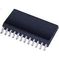
MTS62C19A-HS105 Microchip Technology, MTS62C19A-HS105 Datasheet - Page 4

MTS62C19A-HS105
Manufacturer Part Number
MTS62C19A-HS105
Description
Dual Full-Bridge PWM Motor Driver 24 SOIC .300in TUBE
Manufacturer
Microchip Technology
Type
Dual Full-Bridge Motor Driverr
Datasheet
1.MTS62C19A-HS105.pdf
(18 pages)
Specifications of MTS62C19A-HS105
Product
Stepper Motor Controllers / Drivers
Operating Supply Voltage
10 V to 40 V
Supply Current
0.8 mA
Mounting Style
SMD/SMT
Package / Case
SOIC-24
Operating Temperature
- 20 C to + 85 C
Peak Reflow Compatible (260 C)
Yes
Rohs Compliant
Yes
Motor Type
Full Bridge
No. Of Outputs
2
Output Current
1A
Supply Voltage Range
10V To 40V
Driver Case Style
SOIC
No. Of Pins
24
Operating Temperature Range
-20°C To +85°C
Lead Free Status / RoHS Status
Lead free / RoHS Compliant
Lead Free Status / RoHS Status
Lead free / RoHS Compliant
Other names
MTS62C19A-HS105TR
Available stocks
Company
Part Number
Manufacturer
Quantity
Price
Company:
Part Number:
MTS62C19A-HS105
Manufacturer:
MICROCHIP
Quantity:
12 000
MTS62C19A
1.0
Absolute Maximum Ratings †
Logic Supply Voltage (V
Load Supply Voltage (V
Logic Input Voltage Range (V
V
Output Current (Peak) ..................................................... ±1A
Output Current (Continuous) ...................................... ±0.75A
Sense Output Voltage ...................................... -0.3V to 1.5V
Junction Temperature (T
Operating Temperature Range (T
Storage Temperature Range (T
ELECTRICAL CHARACTERISTICS
DS22260A-page 4
Electrical Specifications: Unless otherwise specified, all limits are established for V
T
DC Characteristics
Logic Supply Voltage
Load Supply Voltage
Logic Supply Current
V
Driver Supply Current
Control Logic Input Current
(V
Logic Low Input Voltage
Logic High Input Voltage
Current Limit Threshold
Ratio (V
Driver Output Saturation
Voltage V
Clamp Diode Forward Volt-
age (Note 2)
Driver Output Leakage Cur-
rent
Thermal Shutdown Temper-
ature
AC Characteristics
Cut-off Time (one-shot
pulse)
Turn-off Delay
Note 1:
REF
A
REF
IN
= 25°C
= 0V)
Voltage Range (V
Voltage Range
2:
Parameters
REF
ELECTRICAL
CHARACTERISTICS
CE(SAT)
÷ V
V
Clamp/Freewheel diode is the intrinsic body-drain diode of the NMOS and PMOS transistors.
IN
SENSE
= 5.0V input current given by internal pull-up to Logic Supply.
)
REF
LOAD
LOGIC
J
).............................-20°C to +150°C
) ............................. -0.3 to +10.0V
) .......................... -0.3 to +40.0V
IN
) ......................... -0.3 to +5.5V
) ....... -0.3 to VLOGIC + 0.3V
STG
V
I
(High Side)
(Low Side)
V
I
V
VLOAD_OFF
REF
VLOAD_ON
OPR
T
F_NDIODE
F_PDIODE
V
I
V
VLOGIC
) .............-55°C to +150°C
V
J_SHDN
V
V
I
Sym
T
LOGIC
LEAK
LOAD
V
V
I
_V
ONN
ONP
T
REF
OFF
IN
E
)............-20°C to +85°C
IL
IH
D
SENS
13.5
25.5
Min
4.5
1.5
2.4
9.5
10
—
—
—
—
—
—
—
—
—
—
—
—
—
—
—
—
0.55
0.55
0.55
0.90
1.05
1.85
0.95
1.00
Typ
170
5.0
0.8
5.0
1.5
30
—
—
—
10
15
30
—
—
50
—
† Notice: Stresses above those listed under “Maximum Rat-
ings” may cause permanent damage to the device. This is a
stress rating only and functional operation of the device at
those or any other conditions above those indicated in the
operational listings of this specification is not implied. Expo-
sure to maximum rating conditions for extended periods may
affect device reliability.
Max
10.5
16.5
34.5
0.65
1.00
1.40
2.10
1.30
1.30
5.5
1.0
7.0
1.0
1.0
-70
0.8
-50
40
50
58
10
—
—
—
Units
LOGIC
mA
mA
mA
µA
µA
µA
°C
µs
µs
—
—
—
V
V
V
V
V
V
V
V
V
V
V
= 4.5V to 5.5V,V
Both Bridges ON, No Load
Both Bridges Off
I01,I11,I02,I12,PHASE1,PHASE2,
(Note 1)
I01,I11,I02,I12,PHASE1,PHASE2
I01,I11,I02,I12,PHASE1,PHASE2
I0=L,I1=L
I0=H,I1=L
I0=L,I1=H
(Sink) IOUT = +500 mA
(Sink) IOUT = +750 mA
(Source) IOUT = -500 mA
(Source) IOUT = -750 mA
I
I
VOUT = 0V
V
Rs=1 ,Rc=1k ,Cc=820pF,
Rt=56k , Ct=820pF
F
F
OUT
= 750 mA
= 750 mA
2010 Microchip Technology Inc.
= V
LOAD
Conditions
LOAD
= 30V,V
REF
= 5V,


