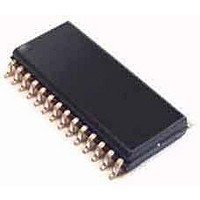
PIC18F26K80T-I/SO Microchip Technology, PIC18F26K80T-I/SO Datasheet - Page 428

PIC18F26K80T-I/SO
Manufacturer Part Number
PIC18F26K80T-I/SO
Description
ECAN, 64KB Flash, 4KB RAM, 16 MIPS, 12-bit ADC, CTMU 28 SOIC .300in T/R
Manufacturer
Microchip Technology
Series
PIC® XLP™ 18Fr
Datasheet
1.PIC18F25K80-ISO.pdf
(628 pages)
Specifications of PIC18F26K80T-I/SO
Core Processor
PIC
Core Size
8-Bit
Speed
64MHz
Connectivity
ECAN, I²C, LIN, SPI, UART/USART
Peripherals
Brown-out Detect/Reset, LVD, POR, PWM, WDT
Number Of I /o
24
Program Memory Size
64KB (32K x 16)
Program Memory Type
FLASH
Eeprom Size
1K x 8
Ram Size
3.6K x 8
Voltage - Supply (vcc/vdd)
1.8 V ~ 5.5 V
Data Converters
A/D 8x12b
Oscillator Type
Internal
Operating Temperature
-40°C ~ 85°C
Package / Case
*
Processor Series
PIC18F26K80
Core
PIC
Data Bus Width
8 bit
Data Ram Size
1 KB
Interface Type
I2C, SPI, USART
Maximum Clock Frequency
64 MHz
Number Of Programmable I/os
24
Number Of Timers
5
Operating Supply Voltage
1.8 V to 5.5 V
Maximum Operating Temperature
+ 85 C
Mounting Style
SMD/SMT
Lead Free Status / RoHS Status
Lead free / RoHS Compliant
Lead Free Status / RoHS Status
Lead free / RoHS Compliant
- Current page: 428 of 628
- Download datasheet (6Mb)
PIC18F66K80 FAMILY
REGISTER 27-45: RXFCONn: RECEIVE FILTER CONTROL REGISTER ‘n’ [0 n 1]
REGISTER 27-46: SDFLC: STANDARD DATA BYTES FILTER LENGTH COUNT REGISTER
DS39977C-page 428
RXFCON0
RXFCON1
Legend:
R = Readable bit
-n = Value at POR
bit 7-0
Note 1:
bit 7
Legend:
R = Readable bit
-n = Value at POR
bit 7-5
bit 4-0
Note 1:
Note:
U-0
—
This register is available in Mode 1 and 2 only.
This register is available in Mode 1 and 2 only.
Register 27-46
bit 7
RXF<7:0>EN: Receive Filter n Enable bits
0 = Filter is disabled
1 = Filter is enabled
RXF15EN
RXF7EN
R/W-0
R/W-0
Unimplemented: Read as ‘ 0 ’
FLC<4:0>: Filter Length Count bits
Mode 0:
Not used; forced to ‘ 00000 ’.
00000 - 10010 = 0
If DLC<3:0>
If DLC<3:0>
If DLC<3:0>
If DLC<3:0>
U-0
—
through
RXF14EN
RXF6EN
R/W-0
R/W-0
W = Writable bit
‘1’ = Bit is set
= 0000 No bits will be compared with incoming data bits.
= 0001 Up to 8 data bits of RXFnEID<7:0>, as determined by FLC<2:0>, will be com-
= 0010 Up to 16 data bits of RXFnEID<15:0>, as determined by FLC<3:0>, will be
= 0011 Up to 18 data bits of RXFnEID<17:0>, as determined by FLC<4:0>, will be
Register 27-51
U-0
—
W = Writable bit
‘1’ = Bit is set
18 bits are available for standard data byte filter. Actual number of bits used
depends on the DLC<3:0> bits (RXBnDLC<3:0> or BnDLC<3:0> if configured
as RX buffer) of the message being received.
pared with the corresponding number of data bits of the incoming message.
compared with the corresponding number of data bits of the incoming
message.
compared with the corresponding number of data bits of the incoming
message.
RXF13EN
RXF5EN
R/W-0
R/W-0
R/W-0
FLC4
Preliminary
are writable in Configuration mode only.
RXF12EN RXF11EN
RXF4EN
R/W-0
R/W-0
U = Unimplemented bit, read as ‘0’
‘0’ = Bit is cleared
R/W-0
FLC3
U = Unimplemented bit, read as ‘0’
‘0’ = Bit is cleared
RXF3EN
R/W-0
R/W-0
R/W-0
FLC2
RXF10EN
RXF2EN
R/W-0
R/W-0
2011 Microchip Technology Inc.
x = Bit is unknown
x = Bit is unknown
R/W-0
FLC1
RXF1EN
RXF9EN
R/W-0
R/W-0
(1)
RXF0EN
RXF8EN
(1)
R/W-0
R/W-0
R/W-0
FLC0
bit 0
bit 0
Related parts for PIC18F26K80T-I/SO
Image
Part Number
Description
Manufacturer
Datasheet
Request
R

Part Number:
Description:
Manufacturer:
Microchip Technology Inc.
Datasheet:

Part Number:
Description:
Manufacturer:
Microchip Technology Inc.
Datasheet:

Part Number:
Description:
Manufacturer:
Microchip Technology Inc.
Datasheet:

Part Number:
Description:
Manufacturer:
Microchip Technology Inc.
Datasheet:

Part Number:
Description:
Manufacturer:
Microchip Technology Inc.
Datasheet:

Part Number:
Description:
Manufacturer:
Microchip Technology Inc.
Datasheet:

Part Number:
Description:
Manufacturer:
Microchip Technology Inc.
Datasheet:

Part Number:
Description:
Manufacturer:
Microchip Technology Inc.
Datasheet:


