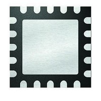
PIC18LF13K22-E/ML Microchip Technology, PIC18LF13K22-E/ML Datasheet - Page 212

PIC18LF13K22-E/ML
Manufacturer Part Number
PIC18LF13K22-E/ML
Description
8KB Flash, 256bytes RAM, 256bytes EEPROM, 16MIPS, NanoWatt XLP 20 QFN 4x4mm TUBE
Manufacturer
Microchip Technology
Series
PIC® XLP™ 18Fr
Datasheets
1.PIC18LF13K22-ISS.pdf
(388 pages)
2.PIC18LF13K22-ISS.pdf
(12 pages)
3.PIC18LF13K22-ISS.pdf
(36 pages)
Specifications of PIC18LF13K22-E/ML
Core Processor
PIC
Core Size
8-Bit
Speed
48MHz
Connectivity
I²C, LIN, SPI, UART/USART
Peripherals
Brown-out Detect/Reset, POR, PWM, WDT
Number Of I /o
17
Program Memory Size
8KB (4K x 16)
Program Memory Type
FLASH
Eeprom Size
256 x 8
Ram Size
256 x 8
Voltage - Supply (vcc/vdd)
1.8 V ~ 3.6 V
Data Converters
A/D 12x10b
Oscillator Type
Internal
Operating Temperature
-40°C ~ 125°C
Package / Case
20-VQFN Exposed Pad, 20-HVQFN, 20-SQFN, 20-DHVQFN
Processor Series
PIC18LF
Core
PIC
Data Bus Width
8 bit
Data Ram Size
256 B
Interface Type
EUSART, I2C, SPI
Maximum Clock Frequency
32 KHz
Number Of Programmable I/os
18
Number Of Timers
4
Operating Supply Voltage
1.8 V to 3.6 V
Maximum Operating Temperature
+ 125 C
Mounting Style
SMD/SMT
3rd Party Development Tools
52715-96, 52716-328, 52717-734, 52712-325, EWPIC18
Development Tools By Supplier
PG164130, DV164035, DV244005, DV164005
Minimum Operating Temperature
- 40 C
On-chip Adc
10 bit, 12 Channel
A/d Bit Size
10 bit
A/d Channels Available
12
Height
0.88 mm
Length
4 mm
Supply Voltage (max)
3.6 V
Supply Voltage (min)
1.8 V, 2.7 V
Width
4 mm
Lead Free Status / RoHS Status
Lead free / RoHS Compliant
Lead Free Status / RoHS Status
Lead free / RoHS Compliant
- Current page: 212 of 388
- Download datasheet (4Mb)
PIC18F1XK22/LF1XK22
16.2.9
This is an example procedure for using the ADC to
perform an Analog-to-Digital conversion:
1.
2.
3.
4.
5.
6.
7.
8.
DS41365D-page 212
Note 1: The global interrupt can be disabled if the
Configure Port:
• Disable pin output driver (See TRIS register)
• Configure pin as analog
Configure the ADC module:
• Select ADC conversion clock
• Configure voltage reference
• Select ADC input channel
• Select result format
• Select acquisition delay
• Turn on ADC module
Configure ADC interrupt (optional):
• Clear ADC interrupt flag
• Enable ADC interrupt
• Enable peripheral interrupt
• Enable global interrupt
Wait the required acquisition time
Start conversion by setting the GO/DONE bit.
Wait for ADC conversion to complete by one of
the following:
• Polling the GO/DONE bit
• Waiting for the ADC interrupt (interrupts
Read ADC Result
Clear the ADC interrupt flag (required if interrupt
is enabled).
enabled)
2: Software delay required if ACQT bits are
A/D CONVERSION PROCEDURE
user is attempting to wake-up from Sleep
and resume in-line code execution.
set to zero delay. See Section 16.3 “A/D
Acquisition Requirements”.
(1)
(2)
.
Preliminary
EXAMPLE 16-1:
;This code block configures the ADC
;for polling, Vdd and Vss as reference, Frc
clock and AN4 input.
;
;Conversion start & polling for completion
; are included.
;
MOVLW
MOVWF
MOVLW
MOVWF
BSF
BSF
MOVLW
MOVWF
BSF
ADCPoll:
BTFSC
BRA
; Result is complete - store 2 MSbits in
; RESULTHI and 8 LSbits in RESULTLO
MOVFF
MOVFF
B’10101111’ ;right justify, Frc,
ADCON2
B’00000000’ ;ADC ref = Vdd,Vss
ADCON1
TRISC,0
ANSEL,4
B’00010001’ ;AN4, ADC on
ADCON0
ADCON0,GO
ADCON0,GO
ADCPoll
ADRESH,RESULTHI
ADRESL,RESULTLO
A/D CONVERSION
2010 Microchip Technology Inc.
; & 12 TAD ACQ time
;
;Set RC0 to input
;Set RC0 to analog
;
;Start conversion
;Is conversion done?
;No, test again
Related parts for PIC18LF13K22-E/ML
Image
Part Number
Description
Manufacturer
Datasheet
Request
R

Part Number:
Description:
Manufacturer:
Microchip Technology Inc.
Datasheet:

Part Number:
Description:
Manufacturer:
Microchip Technology Inc.
Datasheet:

Part Number:
Description:
Manufacturer:
Microchip Technology Inc.
Datasheet:

Part Number:
Description:
Manufacturer:
Microchip Technology Inc.
Datasheet:

Part Number:
Description:
Manufacturer:
Microchip Technology Inc.
Datasheet:

Part Number:
Description:
Manufacturer:
Microchip Technology Inc.
Datasheet:

Part Number:
Description:
Manufacturer:
Microchip Technology Inc.
Datasheet:

Part Number:
Description:
Manufacturer:
Microchip Technology Inc.
Datasheet:


