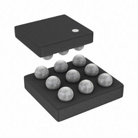
SSM2315CBZ-REEL Analog Devices Inc, SSM2315CBZ-REEL Datasheet - Page 12

SSM2315CBZ-REEL
Manufacturer Part Number
SSM2315CBZ-REEL
Description
IC,Audio Amplifier,SINGLE,BGA,9PIN,PLASTIC
Manufacturer
Analog Devices Inc
Type
Class Dr
Datasheet
1.SSM2315CBZ-REEL7.pdf
(16 pages)
Specifications of SSM2315CBZ-REEL
Output Type
1-Channel (Mono)
Max Output Power X Channels @ Load
4.28W x 1 @ 3 Ohm
Voltage - Supply
2.5 V ~ 5.5 V
Features
Depop, Differential Inputs, Short-Circuit and Thermal Protection, Shutdown
Mounting Type
Surface Mount
Package / Case
9-WLCSP
Lead Free Status / RoHS Status
Lead free / RoHS Compliant
For Use With
SSM2317-EVALZ - BOARD EVAL SSM2317
Lead Free Status / RoHS Status
Lead free / RoHS Compliant
Available stocks
Company
Part Number
Manufacturer
Quantity
Price
Company:
Part Number:
SSM2315CBZ-REEL
Manufacturer:
ADI
Quantity:
26 955
Company:
Part Number:
SSM2315CBZ-REEL7
Manufacturer:
ADI
Quantity:
26 955
Part Number:
SSM2315CBZ-REEL7
Manufacturer:
ADI/亚德诺
Quantity:
20 000
SSM2315
THEORY OF OPERATION
OVERVIEW
The SSM2315 mono Class-D audio amplifier features a filterless
modulation scheme that greatly reduces the external component
count, conserving board space and, thus, reducing systems cost.
The SSM2315 does not require an output filter but, instead, relies
on the inherent inductance of the speaker coil and the natural
filtering of the speaker and human ear to fully recover the audio
component of the square wave output. Most Class-D amplifiers
use some variation of pulse-width modulation (PWM), but the
SSM2315 uses a Σ-Δ modulation to determine the switching
pattern of the output devices, resulting in a number of important
benefits. Σ-Δ modulators do not produce a sharp peak with many
harmonics in the AM frequency band, as pulse-width modulators
often do. Σ-Δ modulation provides the benefits of reducing the
amplitude of spectral components at high frequencies, that is,
reducing EMI emission that may otherwise be radiated by
speakers and long cable traces. The SSM2315 does not require
external EMI filtering for twisted speaker cable lengths shorter
than 10 cm. Due to the inherent spread spectrum nature of Σ-Δ
modulation, the need for oscillator synchronization is eliminated
for designs incorporating multiple SSM2315 amplifiers.
The SSM2315 also offers protection circuits for overcurrent and
temperature protection.
GAIN
The SSM2315 has a default gain of 6 dB that can be reduced by
using a pair of external resistors with a value calculated as follows:
POP-AND-CLICK SUPPRESSION
Voltage transients at the output of audio amplifiers may occur
when shutdown is activated or deactivated. Voltage transients as
low as 10 mV can be heard as an audio pop in the speaker. Clicks
and pops can also be classified as undesirable audible transients
generated by the amplifier system and, therefore, as not coming
from the system input signal. Such transients may be generated
when the amplifier system changes its operating mode. For example,
the following may be sources of audible transients: system power-up
and power-down, mute and unmute, input source change, and
sample rate change. The SSM2315 has a pop-and-click suppression
architecture that reduces these output transients, resulting in
noiseless activation and deactivation.
External Gain Settings = 160 kΩ/(80 kΩ + R
EXT
)
Rev. A | Page 12 of 16
OUTPUT MODULATION DESCRIPTION
The SSM2315 uses three-level, Σ-Δ output modulation. Each
output can swing from GND to VDD and vice versa. Ideally,
when no input signal is present, the output differential voltage
is 0 V because there is no need to generate a pulse. In a real world
situation, there are always noise sources present.
Due to this constant presence of noise, a differential pulse is
generated, when required, in response to this stimulus. A small
amount of current flows into the inductive load when the differen-
tial pulse is generated.
However, most of the time, output differential voltage is 0 V,
due to the Analog Devices patented, three-level, Σ-Δ output
modulation. This feature ensures that the current flowing through
the inductive load is small.
When the user wants to send an input signal, an output pulse
is generated to follow the input voltage. The differential pulse
density is increased by raising the input signal level. Figure 33
depicts three-level, Σ-Δ output modulation with and without
input stimulus.
Figure 33. Three-Level, Σ-Δ Output Modulation With and Without Input Stimulus
OUT+
VOUT
OUT+
VOUT
OUT+
VOUT
OUT–
OUT–
OUT–
OUTPUT = 0V
OUTPUT > 0V
OUTPUT < 0V
+5V
0V
+5V
0V
+5V
0V
–5V
+5V
0V
+5V
0V
+5V
0V
+5V
0V
+5V
0V
0V
–5V


