SSM2356CBZ-RL Analog Devices Inc, SSM2356CBZ-RL Datasheet
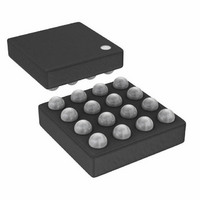
2x2W Filterless Class D Stereo Audio Amp

SSM2356CBZ-RL

Manufacturer Part Number
SSM2356CBZ-RL
Description
2x2W Filterless Class D Stereo Audio Amp
Manufacturer
Analog Devices Inc
Type
Class Dr
Datasheet

Specifications of SSM2356CBZ-RL

Output Type
2-Channel (Stereo)
Max Output Power X Channels @ Load
2.5W x 2 @ 4 Ohm
Voltage - Supply
2.5 V ~ 5.5 V
Features
Depop, Differential Inputs, Short-Circuit and Thermal Protection, Shutdown
Mounting Type
Surface Mount
Package / Case
16-WLCSP
Lead Free Status / RoHS Status
Lead free / RoHS Compliant
FEATURES
Filterless stereo Class-D amplifier with Σ-Δ modulation
No sync necessary when using multiple Class-D amplifiers
2 × 2W into 4 Ω load and 2x1.4 W into 8 Ω load at 5.0 V
92% efficiency at 5.0 V, 1.4 W into 8 Ω speaker
>103 dB signal-to-noise ratio (SNR)
Single-supply operation from 2.5 V to 5.5 V
20 nA shutdown current; left/right channel control
Short-circuit and thermal protection
Available in a 16-ball, 1.66 mm × 1.66 mm WLCSP
Pop-and-click suppression
Built-in resistors that reduce board component count
User-selectable 6 dB or 18 dB gain setting
User-selectable ultralow EMI emission mode
APPLICATIONS
Mobile phones
MP3 players
Portable gaming
Portable electronics
GENERAL DESCRIPTION
The SSM2356 is a fully integrated, high efficiency, stereo Class-D
audio amplifier. It is designed to maximize performance for
mobile phone applications. The application circuit requires
a minimum of external components and operates from a single
2.5 V to 5.5 V supply. It is capable of delivering 2 × 2W of contin-
uous output power with <1% THD + N driving a 4 Ω load from a
5.0 V supply.
Rev. 0
Information furnished by Analog Devices is believed to be accurate and reliable. However, no
responsibility is assumed by Analog Devices for its use, nor for any infringements of patents or other
rights of third parties that may result from its use. Specifications subject to change without notice. No
license is granted by implication or otherwise under any patent or patent rights of Analog Devices.
Trademarks and registered trademarks are the property of their respective owners.
from Analog Devices, Inc.
supply with <1% total harmonic distortion (THD + N)
SHUTDOWN–R
SHUTDOWN–L
1
RIGHT IN+
RIGHT IN–
INPUT CAPS ARE OPTIONAL IF INPUT DC COMMON-MODE
VOLTAGE IS APPROXIMATELY V
LEFT IN+
LEFT IN–
22nF
22nF
22nF
22nF
GAIN
1
1
1
1
INR+
INR–
SDNR
SDNL
INL+
INL–
SSM2356
FUNCTIONAL BLOCK DIAGRAM
80kΩ
80kΩ
80kΩ
80kΩ
DD
GAIN
/2.
CONTROL
CONTROL
GAIN
GAIN
GAIN = 6dB OR 18dB
10µF
Figure 1.
BIAS
BIAS
MODULATOR
MODULATOR
0.1µF
OSCILLATOR
(Σ-Δ)
(Σ-Δ)
INTERNAL
One Technology Way, P.O. Box 9106, Norwood, MA 02062-9106, U.S.A.
Tel: 781.329.4700
Fax: 781.461.3113
The SSM2356 features a high efficiency, low noise modulation
scheme that requires no external LC output filters. The modulation
continues to provide high efficiency even at low output power.
It operates with 92% efficiency at 1.4 W into 8 Ω or 85% efficiency
at 2.0 W into 4 Ω from a 5.0 V supply and has an SNR of >103 dB.
Spread-spectrum pulse density modulation is used to provide
lower EMI-radiated emissions compared with other Class-D
architectures. The SSM2356 includes an optional modulation
select pin (ultralow EMI emission mode) that significantly
reduces the radiated emissions at the Class-D outputs, particularly
above 100 MHz.
The SSM2356 has a micropower shutdown mode with a typical
shutdown current of 20 nA. Shutdown is enabled by applying
a logic low to the SDNR and SDNL pins. The device also
includes pop-and-click suppression circuitry that minimizes
voltage glitches at the output during turn-on and turn-off,
reducing audible noise on activation and deactivation.
The fully differential input of the SSM2356 provides excellent
rejection of common-mode noise on the input. Input coupling
capacitors can be omitted if the dc input common-mode voltage
is approximately V
selected between 6 dB and 18 dB with no external components
and no change to the input impedance. Gain can be further
reduced to a user-defined setting by inserting series external
resistors at the inputs.
The SSM2356 is specified over the commercial temperature range
(−40°C to +85°C). It has built-in thermal shutdown and output
short-circuit protection. It is available in a 16-ball, 1.66 mm ×
1.66 mm wafer level chip scale package (WLCSP).
VDD
GND
VDD
2 × 2W Filterless Class-D
DRIVER
DRIVER
CONTROL
FET
FET
VBATT
2.5V TO 5.5V
GND
EDGE
Stereo Audio Amplifier
DD
OUTR+
OUTR–
/2. The preset gain of SSM2356 can be
OUTL+
OUTL–
EDGE
©2009 Analog Devices, Inc. All rights reserved.
EMISSION
CTRL
SSM2356
www.analog.com

Related parts for SSM2356CBZ-RL

SSM2356CBZ-RL Summary of contents

Page 1

FEATURES Filterless stereo Class-D amplifier with Σ-Δ modulation No sync necessary when using multiple Class-D amplifiers from Analog Devices, Inc. 2 × 2W into 4 Ω load and 2x1.4 W into 8 Ω load at 5.0 V supply with <1% ...

Page 2

SSM2356 TABLE OF CONTENTS Features .............................................................................................. 1 Applications ....................................................................................... 1 General Description ......................................................................... 1 Functional Block Diagram .............................................................. 1 Revision History ............................................................................... 2 Specifications ..................................................................................... 3 Absolute Maximum Ratings ............................................................ 4 Thermal Resistance ...................................................................... 4 ESD Caution .................................................................................. 4 Pin ...

Page 3

SPECIFICATIONS 5 Ω +33 μH, EDGE = GND, Gain = 6 dB, unless otherwise noted Table 1. Parameter DEVICE CHARACTERISTICS Output Power/Channel Efficiency Total Harmonic Distortion ...

Page 4

SSM2356 ABSOLUTE MAXIMUM RATINGS Absolute maximum ratings apply at 25°C, unless otherwise noted. Table 2. Parameter Supply Voltage Input Voltage Common-Mode Input Voltage ESD Susceptibility Storage Temperature Range Operating Temperature Range Junction Temperature Range Lead Temperature Range (Soldering, 60 sec) ...

Page 5

PIN CONFIGURATION AND FUNCTION DESCRIPTIONS Table 4. Pin Function Descriptions Bump Mnemonic Description A1 OUTL+ Noninverting Output for Left Channel. B1 OUTL− Inverting Output for Left Channel. C1 SDNL Shutdown, Left Channel. Active low digital input. D1 INL+ Noninverting Input ...

Page 6

SSM2356 TYPICAL PERFORMANCE CHARACTERISTICS 100 R = 8Ω + 33µH L GAIN = 6dB 0.1 0.01 0.001 0.0001 0.001 0.01 0.1 OUTPUT POWER (W) Figure 3. THD + N vs. Output Power into 8 ...

Page 7

GAIN = 6dB R = 4Ω + 15µ 0.1 0.01 1W 0.001 10 100 1k FREQUENCY (Hz) Figure 9. THD + N vs. Frequency ...

Page 8

SSM2356 100 V = 2.5V DD GAIN = 6dB R = 8Ω + 33µ 0.25W 0.1 0.0625W 0.01 0.125W 0.001 10 100 1k FREQUENCY (Hz) Figure 15. THD + N vs. Frequency 2 ...

Page 9

GAIN = 6dB 1 8Ω + 33µH L 1.6 1.4 1.2 10% 1.0 0.8 1% 0.6 0.4 0.2 0 2.5 3.0 3.5 4.0 SUPPLY VOLTAGE (V) Figure 21. Maximum Output Power vs. Supply Voltage, ...

Page 10

SSM2356 0.8 GAIN = 6dB R = 8Ω + 33µ FOR BOTH CHANNELS SY OUT 0 3.6V 0 2.5V DD 0.3 0.2 0 0.5 1.0 1.5 2.0 ...

Page 11

OUTPUT –1 SD INPUT –2 –110 –90 –70 –50 –30 – TIME (µs) Figure 33. Turn-Off Response 50 70 Rev Page SSM2356 ...

Page 12

SSM2356 TYPICAL APPLICATION CIRCUITS 22nF RIGHT AUDIO IN+ RIGHT AUDIO IN– 22nF SHUTDOWN–R SHUTDOWN–L 22nF LEFT AUDIO IN+ LEFT AUDIO IN– 22nF 22nF RIGHT AUDIO IN+ 22nF SHUTDOWN–R SHUTDOWN–L 22nF LEFT AUDIO IN+ 22nF 10µF 0.1µF VDD SSM2356 R 80kΩ ...

Page 13

APPLICATIONS INFORMATION OVERVIEW The SSM2356 stereo Class-D audio amplifier features a filterless modulation scheme that greatly reduces the external component count, conserving board space and, thus, reducing systems cost. The SSM2356 does not require an output filter but, instead, relies ...

Page 14

SSM2356 The measurements for Figure 36 and Figure 37 were taken in an FCC-certified EMI laboratory with a 1 kHz input signal, producing 0.5 W output power into an 8 Ω load from supply. Cable length was ...

Page 15

... OUTLINE DIMENSIONS 1.700 1.660 SQ 1.620 BALL A1 IDENTIFIER TOP VIEW (BALL SIDE DOWN) ORDERING GUIDE Model Temperature Range 1 SSM2356CBZ-REEL −40°C to +85°C 1 SSM2356CBZ-REEL7 −40°C to +85°C 1 EVAL-SSM2356Z RoHS Compliant Part. 0.660 0.600 0.540 SEATING PLANE 0.290 BSC 0.260 0.230 0.07 ...

Page 16

SSM2356 NOTES ©2009 Analog Devices, Inc. All rights reserved. Trademarks and registered trademarks are the property of their respective owners. D08084-0-5/09(0) Rev Page ...

Related keywords