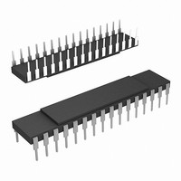
STK14C88-C45I Cypress Semiconductor Corp, STK14C88-C45I Datasheet - Page 4

STK14C88-C45I
Manufacturer Part Number
STK14C88-C45I
Description
STK14C88-C45I
Manufacturer
Cypress Semiconductor Corp
Datasheet
1.STK14C88-C45I.pdf
(19 pages)
Specifications of STK14C88-C45I
Format - Memory
RAM
Memory Type
NVSRAM (Non-Volatile SRAM)
Memory Size
256K (32K x 8)
Speed
45ns
Interface
Parallel
Voltage - Supply
4.5 V ~ 5.5 V
Operating Temperature
-40°C ~ 85°C
Package / Case
32-CDIP (0.300", 7.62mm)
Lead Free Status / RoHS Status
Contains lead / RoHS non-compliant
Available stocks
Company
Part Number
Manufacturer
Quantity
Price
Company:
Part Number:
STK14C88-C45I
Manufacturer:
a
Quantity:
2
Absolute Maximum Ratings
Voltage on Input Relative to Ground.................–0.5V to 7.0V
Voltage on Input Relative to V
Voltage on DQ
Temperature under Bias ............................... –55°C to 125°C
Storage Temperature .................................... –65°C to 150°C
Power Dissipation............................................................. 1W
DC Output Current (1 output at a time, 1s duration).... 15 mA
DC Characteristics
Over the operating range (V
Notes
Document Number: 001-52038 Rev. *B
I
I
I
I
I
I
I
I
V
V
V
V
V
T
1. I
2. I
3. E ≥ V
4. V
CC 1
CC 2
CC 3
CC 4
SB 1
SB 2
ILK
OLK
A
IH
IL
OH
OL
BL
Symbol
CC1
CC2
[3]
[3]
[1]
[2]
[1]
[2]
CC
and I
and I
reference levels throughout this data sheet refer to V
IH
does not produce standby current levels until any nonvolatile cycle in progress has timed out.
CC3
CC4
Average V
Average V
STORE
Average V
200 ns
5V, 25°C, Typical
Average V
AutoStore Cycle
Average V
(Standby, Cycling TTL Input
Levels)
V
(Standby, Stable CMOS Input
Levels)
Input Leakage Current
Off-State Output Leakage Current
Input Logic “1” Voltage
Input Logic “0” Voltage
Output Logic “1” Voltage
Output Logic “0” Voltage
Logic “0” Voltage on HSB Output
Operating Temperature
are dependent on output loading and cycle rate. The specified values are obtained with outputs unloaded.
are the average currents required for the duration of the respective STORE cycles (t
0-7
CC
or HSB ......................–0.5V to (V
Standby Current
CC
CC
CC
CAP
CC
Parameter
CC
Current at t
Current
Current
Current during
Current during
SS
= 5.0V ± 10%)
...........–0.6V to (V
AVAV
=
[4]
CC
CC
CC
V
if that is where the power supply connection is made, or V
SS
Min
2.2
2.4
+ 0.5V)
+ 0.5V)
0
Commercial
– .5
V
CC
Max
1.5
0.8
0.4
0.4
97
80
70
10
30
25
22
±1
±5
70
3
2
+ 0.5
Note Stresses greater than those listed under “Absolute
Maximum Ratings” may cause permanent damage to the device.
This is a stress rating only, and functional operation of the device
at conditions above those indicated in the operational sections
of this specification is not implied. Exposure to absolute
maximum rating conditions for extended periods may affect
reliability.
V
-40/-55
SS
Min
2.2
2.4
Industrial/
– .5
Military
STORE
V
85/125
CC
Max
).
100
1.5
0.8
0.4
0.4
85
70
10
31
26
23
±1
±5
3
2
+0.5
Unit
mA
mA
mA
mA
mA
mA
mA
mA
mA
mA
μA
μA
°C
CAP
V
V
V
V
V
if V
CC
t
t
t
All Inputs Don’t Care, V
max
W ≥ (V
All Others Cycling, CMOS
Levels
All Inputs Don’t Care
t
t
t
E ≥ (V
All Others V
– 0.2V)
V
V
V
V
All Inputs
All Inputs
I
I
I
AVAV
AVAV
AVAV
AVAV
AVAV
AVAV
OUT
OUT
OUT
CC
IN
CC
IN
is connected to ground.
= V
= V
= max
= max
= – 4 mA except HSB
= 8 mA except HSB
= 3 mA
= 25 ns
= 35 ns
= 45 ns
= 25 ns, E ≥ V
= 35 ns, E ≥ V
= 45 ns, E ≥ V
CC
SS
CC
SS
– 0.2V)
to V
– 0.2V)
to V
STK14C88
IN
Notes
≤ 0.2V or ≥ (V
CC
CC
, E or G ≥ V
Page 4 of 19
IH
IH
IH
CC
=
CC
IH
[+] Feedback
[+] Feedback
[+] Feedback


