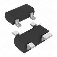
TC1270ARVRCTR Microchip Technology, TC1270ARVRCTR Datasheet - Page 20

TC1270ARVRCTR
Manufacturer Part Number
TC1270ARVRCTR
Description
IC,Power Supply Supervisor,TO-253,4PIN,PLASTIC
Manufacturer
Microchip Technology
Type
Simple Reset/Power-On Resetr
Datasheet
1.TC1270ALVRCTR.pdf
(48 pages)
Specifications of TC1270ARVRCTR
Number Of Voltages Monitored
1
Output
Push-Pull, Totem Pole
Reset
Active Low
Reset Timeout
140 ms Minimum
Voltage - Threshold
2.63V
Operating Temperature
-40°C ~ 125°C
Mounting Type
Surface Mount
Package / Case
SOT-143, SOT-143B, TO-253AA
Lead Free Status / RoHS Status
Lead free / RoHS Compliant
Available stocks
Company
Part Number
Manufacturer
Quantity
Price
Company:
Part Number:
TC1270ARVRCTR
Manufacturer:
MICROCHIP
Quantity:
12 000
Part Number:
TC1270ARVRCTR
Manufacturer:
MICROCHIP/微芯
Quantity:
20 000
TC1270A/70AN/71A
FIGURE 4-4:
FIGURE 4-5:
FIGURE 4-6:
DS22035C-page 20
MR
MR
MR
+
–
+
–
+
–
Noise Filter
Noise Filter
Noise Filter
Comparator
Comparator
Comparator
Reference
Voltage
Reference
Voltage
Reference
Voltage
TC1270A Block Diagram.
TC1270AN Block Diagram.
TC1271A Block Diagram.
V
V
V
DD
DD
DD
(Open-
Output
(Push-
Output
Output
(Push-
Drain)
Driver
Delay
Driver
Delay
Driver
Delay
Pull)
Pull)
RST
RST
RST
V
SS
4.2
The voltage detect circuit monitors V
Reset voltage trip point (V
device is ordered. The voltage on the device’s V
determines the output state of the RST/RST pin.
V
pin inactive. V
the RST/RST pin active. The state of the RST/RST pin
is unknown for V
V
TABLE 4-1:
The term V
trip point voltage where the device actually trips.
In the case where V
above V
• Voltages above V
• Voltages below V
In the case where V
below V
• Voltages above V
Legend: H = Driven High
Note 1:
V
V
V
DD
TRIP(MIN)
RST/RST output pin to be driven active.
RST/RST output pin to be driven active.
RST/RST output pin to be driven inactive, (or
floated, in the TC1270AN) after the Reset Delay
Timer (t
DD
TRIP(MIN)
DD
voltages above the V
V
V
V
2:
TRIP(MIN)
DD
TRIP(MAX)
Voltage Detect Circuit
TRIP(MAX)
TRIP(MIN)
RST
. This is shown in
TRIP
Voltage Level
U = Unknown, driven either High or Low
The RST/RST pin will be driven inactive
after the Reset Delay Timer (t
out.
The TC1270AN RST pin will be floated
after the Reset Delay Timer (t
out.
< V
), times out.
DD
DD
will be used as the general term for the
):
DD
):
voltages below the V
V
OUTPUT STATES
< V
TRIP(MIN)
DD
TRIP(MAX)
TRIP(MAX)
voltages between V
DD
DD
TRIP(MAX)
LEVELS TO RST/RST
2010 Microchip Technology Inc.
is falling (for voltages starting
is rising (for voltages starting
TRIP(MAX)
TRIP
Table 4-1
will always cause the
will never cause the
will always cause the
) is selected when the
L = Driven Low
H
force the RST/RST
RST
Output State
(1, 2)
U
DD
L
TRIP(MIN)
. The device’s
TRIP(MAX)
RST
RST
) times
) times
RST
L
DD
U
H
(1)
force
and
pin


