PDSP1881 OSRAM Opto Semiconductors Inc, PDSP1881 Datasheet - Page 7
PDSP1881
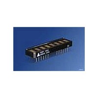
Manufacturer Part Number
PDSP1881
Description
LED Displays 5x7 Yellow 0.18 , 8-CHARACTER
Manufacturer
OSRAM Opto Semiconductors Inc
Series
Alphanumeric Programmable Display™r
Datasheet
1.PDSP1880.pdf
(15 pages)
Specifications of PDSP1881
Display Type
Dot Matrix
Emitting Color
Yellow
Number Of Digits
8
Digit Size (in)
.18in
Viewing Area Height (mm)
4.57mm
Viewing Area Length (mm)
2.54mm
Package Type
Panel
Operating Supply Voltage (min)
4.5V
Operating Supply Voltage (typ)
5V
Operating Supply Voltage (max)
5.5V
Operating Temperature Classification
Industrial
Operating Temp Range
-40C to 85C
Mounting
Through Hole
Pin Count
24
Total Thickness (mm)
5.33mm
Opto Display Type
Panel
Pattern Type
Dot Matrix
Millicandela Rating
205µcd
Size / Dimension
1.69" L x 0.45" W x 0.21" H (42.93mm x 11.43mm x 5.33mm)
Color
Yellow
Configuration
5 x 7
Character Size
0.18 in
Illumination Color
Yellow
Wavelength
583 nm
Maximum Operating Temperature
+ 85 C
Minimum Operating Temperature
- 40 C
Luminous Intensity
205 ucd
Viewing Area (w X H)
2.54 mm x 4.57 mm
Lead Free Status / RoHS Status
Compliant
Voltage - Forward (vf) Typ
-
Internal Connection
-
Lead Free Status / Rohs Status
Details
Other names
Q68000A9106
Available stocks
Company
Part Number
Manufacturer
Quantity
Price


Top View
Pin Assignments
Pin #
1
2
3
4
5
6
7–9
10
11
12
13
14
15
2006-03-30
0
Name
Reset
Flash
Address
input
Address
input
No pins
Address
input
Clock
Select
Clock
In/Out
Write
Chip
Enable
Positive
supply
1
Symbol
RST
FL
A0
A1
A2
A3
—
A4
CLS
CLK
WR
CE
V
CC
2
3
Definition
Initializes display; clears Character
RAM (20H), Flash RAM (00H),
control word (00H), and resets
internal counters. UDC Address
Register and UDC RAM
unaffected.
Accesses Flash RAM. Address
inputs A0–A2 select digit address
while data bit D0 sets (D0=1) or
resets (D0=0) Flash bit, A3 and A4
ignored.
A0–A2 select specific digits.
See Table „Memory Selection“
(page 9).
Same as A0
Same as A0
A3 and A4 access parts of memory
together with Flash pin. See Table
1.
No connections
Same as A3
Selects internal or external clock
source. CLS=1 selects internal
clock (master), CLS=0 selects
external clock (slave operation).
Inputs or outputs clock as
determined by CLS.
Writes data into display when
WR=0. Note CE=0 to enable write
cycle.
Enables display’s write and read
cycles when CE=0.
Positive power supply input.
PDSP1880, PDSP1881, PDSP1882, PDSP1883, PDSP1884
4
5
6
IDPA5110
7
7
Pin Assignments
Pin #
16
17
18
19
20
21
22–24 No pins
25
26
27
28
29
30
Cascading Displays
The PDSP188X is designed to drive up to 16 other
PDSP188Xs with input loading of 15 pF each.
General requirements for cascading 16 displays
together:
• Determine the correct address for each display.
• Use CE from an address decoder to select the correct
• Use CE from an address decoder to select the correct
• Select one of the Displays to provide the Clock for the
• Tie CLKSEL to ground on other displays.
• Use RST to synchronize the blinking between the dis-
display.
display.
other displays. Connect CLKSEL to V
play.
plays.
Name
Supply
ground
—
Logic
ground
Read
Data bit
zero
Data bit
one
Data bit
two
Data bit
three
Data bit
four
Data bit
five
Data bit
six
Data bit
seven
Symbol
GND
NC
GND
RD
D0
D1
—
D2
D3
D4
D5
D6
D7
sup
log
Definition
Analog ground for LED drivers
No connection
Logic ground for digital
circuitry
Reads data from display when
RD=0. Also CE=0.
Least significant data bit.
Second data bit.
No connections
Third data bit.
Fourth data bit.
Fifth data bit.
Sixth data bit.
Seventh data bit.
Most significant data bit.
CC
for this dis-
Related parts for PDSP1881
Image
Part Number
Description
Manufacturer
Datasheet
Request
R

Part Number:
Description:
INTELLIGENT DISP 4CHAR 5X7 HERED
Manufacturer:
OSRAM Opto Semiconductors Inc
Datasheet:

Part Number:
Description:
DISPLAY 8DIGIT CERAMIC GREEN
Manufacturer:
OSRAM Opto Semiconductors Inc
Datasheet:

Part Number:
Description:
EMITTER IR 950NM 5MM SMD RADIAL
Manufacturer:
OSRAM Opto Semiconductors Inc
Datasheet:

Part Number:
Description:
LED TOPLED GREEN 570NM 2-PLCC
Manufacturer:
OSRAM Opto Semiconductors Inc
Datasheet:

Part Number:
Description:
INTERRUPTER RELFECT W/FILTR SMD
Manufacturer:
OSRAM Opto Semiconductors Inc
Datasheet:

Part Number:
Description:
LED Displays 5x7 Green 0.145 , 4-CHARACTER
Manufacturer:
OSRAM Opto Semiconductors Inc
Datasheet:

Part Number:
Description:
Q65110A4321_SIDELED PURE GREEN EOL150407
Manufacturer:
OSRAM Opto Semiconductors Inc
Datasheet:
Part Number:
Description:
Q65110A1202_RO DETECTOR 3/5MM_TR_RO
Manufacturer:
OSRAM Opto Semiconductors Inc
Datasheet:

Part Number:
Description:
PHOTODIODE 900NM 3MM W/FILTER
Manufacturer:
OSRAM Opto Semiconductors Inc
Datasheet:
Part Number:
Description:
INTELLIGENT DISP 4CHAR 5X7 HERED
Manufacturer:
OSRAM Opto Semiconductors Inc
Datasheet:
Part Number:
Description:
LED TOPLED GREEN 570NM 2-PLCC
Manufacturer:
OSRAM Opto Semiconductors Inc
Datasheet:
Part Number:
Description:
PHOTODIODE 900NM 3MM W/FILTER
Manufacturer:
OSRAM Opto Semiconductors Inc
Datasheet:

Part Number:
Description:
PHOTODIODE 850NM THRU-HOLE
Manufacturer:
OSRAM Opto Semiconductors Inc
Datasheet:

Part Number:
Description:
PHOTODIODE 880NM W/FILTER SMD
Manufacturer:
OSRAM Opto Semiconductors Inc
Datasheet: