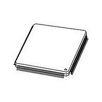
LH79525N0Q100A1 Sharp Electronics, LH79525N0Q100A1 Datasheet - Page 44

LH79525N0Q100A1
Manufacturer Part Number
LH79525N0Q100A1
Description
Manufacturer
Sharp Electronics
Datasheet
1.LH79525N0Q100A1.pdf
(64 pages)
Specifications of LH79525N0Q100A1
Operating Temperature (min)
-40C
Operating Temperature (max)
85C
Applications
Embedded Control
Processing Unit
Microcontroller
Operating Supply Voltage (min)
1.7/3V
Operating Supply Voltage (typ)
1.8/3.3V
Operating Supply Voltage (max)
1.9/3.6V
Package Type
LQFP
Screening Level
Industrial
Pin Count
176
Mounting
Surface Mount
Rad Hardened
No
Lead Free Status / RoHS Status
Compliant
Available stocks
Company
Part Number
Manufacturer
Quantity
Price
Company:
Part Number:
LH79525N0Q100A1
Manufacturer:
FREESCALE
Quantity:
101
Company:
Part Number:
LH79525N0Q100A1,55
Manufacturer:
NXP Semiconductors
Quantity:
10 000
LH79524/LH79525
External DMA Handshake Signal Timing
DREQ TIMING
to HIGH again until after nDACK has been asserted.
44
NOTE: * HCLK is an internal signal provided for reference only.
NOTE: tDREQ0L = DREQ0 LOW Pulse Width = 2 HCLK MIN.
Once asserted, DREQ must not transition from LOW
DEOT0/DEOT1
(See Note)
tDREQ1L = DREQ1 LOW Pulse Width = 2 HCLK MIN.
nBLE[1:0]
nDACK1
DACK0/
D[31:0]
A[23:0]
nWEN
HCLK
nCSx
nOE
Figure 24. Read, from Peripheral to Memory, Burst Size = 1
nDACK1
DREQ0,
DREQ1
DACK0
Figure 23. DREQ Timing Restrictions
Rev. 02 — 17 March 2009
NXP Semiconductors
TRANSITON
MUST NOT
DREQ
TRANSITON
DREQ MAY
DACK/DEOT TIMING
DEOT occur in relation to an external bus access to/from
the external peripheral that requested the DMA transfer.
single read or the last word of a burst read from the
requesting peripheral. The remaining diagrams show
timing for data transfers.
These timing diagrams indicate when nDACK and
The first diagram shows the timing with relation to a
ADDRESS
tDREQ0L,
tDREQ1L
DATA
Product data sheet
System-on-Chip
LH79525-5
LH79525-6


