MC14008BCP ON Semiconductor, MC14008BCP Datasheet

MC14008BCP

Manufacturer Part Number
MC14008BCP
Description
Manufacturer
ON Semiconductor
Datasheet

Specifications of MC14008BCP

Logic Family
4000
Logical Function
Binary Full Adder
Technology
CMOS
Number Of Elements
1
Number Of Bits
4
Propagation Delay Time
800ns
High Level Output Current
-4.2mA
Low Level Output Current
4.2mA
Package Type
PDIP
Operating Supply Voltage (typ)
3.3/5/9/12/15V
Operating Temp Range
-55C to 125C
Operating Supply Voltage (min)
3V
Operating Supply Voltage (max)
18V
Quiescent Current
20uA
Pin Count
16
Mounting
Through Hole
Operating Temperature Classification
Military
Lead Free Status / RoHS Status
Not Compliant

Available stocks

Company
Part Number
Manufacturer
Quantity
Price
Part Number:
MC14008BCP
Manufacturer:
MOTOROLA
Quantity:
6 225
Part Number:
MC14008BCP
Manufacturer:
MOT
Quantity:
1 000
Part Number:
MC14008BCP
Manufacturer:
ON/安森美
Quantity:
20 000
MC14008B
4−Bit Full Adder
P−Channel and N−Channel enhancement mode devices in a single
monolithic structure. This device consists of four full adders with fast
internal look−ahead carry output. It is useful in binary addition and
other arithmetic applications. The fast parallel carry output bit allows
high−speed operation when used with other adders in a system.
Features
Maximum ratings are those values beyond which device damage can occur.
Maximum ratings applied to the device are individual stress limit values (not
normal operating conditions) and are not valid simultaneously. If these limits are
exceeded, device functional operation is not implied, damage may occur and
reliability may be affected.
1. Temperature Derating:
static voltages or electric fields. However, precautions must be taken to avoid
applications of any voltage higher than maximum rated voltages to this
high−impedance circuit. For proper operation, V
to the range V
(e.g., either V
*For additional information on our Pb−Free strategy and soldering details, please
MAXIMUM RATINGS
© Semiconductor Components Industries, LLC, 2005
August, 2005 − Rev. 6
Symbol
V
download the ON Semiconductor Soldering and Mounting Techniques
Reference Manual, SOLDERRM/D.
I
The MC14008B 4−bit full adder is constructed with MOS
in
This device contains protection circuitry to guard against damage due to high
Unused inputs must always be tied to an appropriate logic voltage level
Low−Power Schottky TTL Load Over the Rated Temperature Range
in
Look−Ahead Carry Output
Diode Protection on All Inputs
All Outputs Buffered
Supply Voltage Range = 3.0 Vdc to 18 Vdc
Capable of Driving Two Low−Power TTL Loads or One
Pin−for−Pin Replacement for CD4008B
Pb−Free Packages are Available*
V
T
Plastic “P and D/DW” Packages: – 7.0 mW/_C From 65_C To 125_C
P
, V
, I
T
T
stg
DD
A
D
L
out
out
DC Supply Voltage Range
Input or Output Voltage Range
Input or Output Current
Power Dissipation, per Package
Ambient Temperature Range
Storage Temperature Range
Lead Temperature
SS
SS
(DC or Transient)
(DC or Transient) per Pin
(Note 1)
(8−Second Soldering)
or V
v (V
DD
in
). Unused outputs must be left open.
Parameter
or V
(Voltages Referenced to V
out
) v V
DD
.
in
and V
−0.5 to V
SS
−0.5 to +18.0
−55 to +125
−65 to +150
out
)
Value
± 10
500
260
should be constrained
DD
+ 0.5
1
Unit
mW
mA
°C
°C
°C
V
V
See detailed ordering and shipping information in the package
dimensions section on page 2 of this data sheet.
ORDERING INFORMATION
A
WL, L
YY, Y
WW, W
G
http://onsemi.com
CASE 751B
CASE 648
P SUFFIX
D SUFFIX
PDIP−16
SOIC−16
= Assembly Location
= Wafer Lot
= Year
= Work Week
= Pb−Free Indicator
Publication Order Number:
16
1
16
1
DIAGRAMS
MARKING
MC14008BCP
AWLYYWWG
AWLYWW
MC14008B/D
14008BG

Related parts for MC14008BCP

MC14008BCP Summary of contents

Page 1

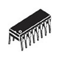
... See detailed ordering and shipping information in the package −65 to +150 dimensions section on page 2 of this data sheet. °C 260 and V should be constrained in out 1 http://onsemi.com MARKING DIAGRAMS 16 PDIP−16 MC14008BCP P SUFFIX AWLYYWWG CASE 648 1 16 SOIC−16 14008BG D SUFFIX AWLYWW CASE 751B Assembly Location WL, L ...

Page 2

PIN ASSIGNMENT ...

Page 3

ELECTRICAL CHARACTERISTICS Î Î Î Î Î ...

Page 4

SWITCHING CHARACTERISTICS (Note 5) Î Î Î ...

Page 5

Figure 3. Dynamic Power Dissipation Test Circuit and Waveform PULSE GENERATOR − out Figure 4. Switching Time Test Circuit and Waveforms MC14008B V ...

Page 6

MC14008B Figure 5. Logic Diagram TYPICAL APPLICATION CHIP CHIP out Calculation of 16−bit adder speed: t total ...

Page 7

−T− 0.25 (0.010 MC14008B PACKAGE DIMENSIONS PDIP−16 P SUFFIX PLASTIC DIP PACKAGE CASE 648−08 ISSUE T L SEATING PLANE ...

Page 8

... American Technical Support: 800−282−9855 Toll Free USA/Canada Japan: ON Semiconductor, Japan Customer Focus Center 2−9−1 Kamimeguro, Meguro−ku, Tokyo, Japan 153−0051 Phone: 81−3−5773−3850 http://onsemi.com 8 NOTES: 1. DIMENSIONING AND TOLERANCING PER ANSI Y14.5M, 1982. 2. CONTROLLING DIMENSION: MILLIMETER. ...

Related keywords