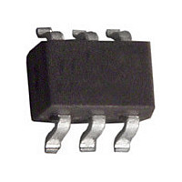
2N7002DW-7-F Diodes Zetex, 2N7002DW-7-F Datasheet - Page 2

2N7002DW-7-F
Manufacturer Part Number
2N7002DW-7-F
Description
MOSFET N-CHAN DUAL 60V SOT363
Manufacturer
Diodes Zetex
Type
Small Signalr
Datasheet
1.2N7002DW-7-F.pdf
(4 pages)
Specifications of 2N7002DW-7-F
Number Of Elements
2
Polarity
N
Channel Mode
Enhancement
Drain-source On-res
7.5Ohm
Drain-source On-volt
60V
Gate-source Voltage (max)
±20V
Drain Current (max)
115mA
Output Power (max)
Not RequiredW
Frequency (max)
Not RequiredMHz
Noise Figure
Not RequireddB
Power Gain
Not RequireddB
Drain Efficiency
Not Required%
Operating Temp Range
-55C to 150C
Operating Temperature Classification
Military
Mounting
Surface Mount
Pin Count
6
Package Type
SOT-363
Power Dissipation
200mW
Continuous Drain Current
115mA
Lead Free Status / RoHS Status
Compliant
Available stocks
Company
Part Number
Manufacturer
Quantity
Price
Company:
Part Number:
2N7002DW-7-F
Manufacturer:
DIODES
Quantity:
36 000
Company:
Part Number:
2N7002DW-7-F
Manufacturer:
DIO
Quantity:
255 000
Company:
Part Number:
2N7002DW-7-F
Manufacturer:
DIODES
Quantity:
2 774
Company:
Part Number:
2N7002DW-7-F
Manufacturer:
DIODES
Quantity:
6 000
Part Number:
2N7002DW-7-F
Manufacturer:
DIODES/美台
Quantity:
20 000
Electrical Characteristics
OFF CHARACTERISTICS (Note 5)
Drain-Source Breakdown Voltage
Zero Gate Voltage Drain Current
Gate-Body Leakage
ON CHARACTERISTICS (Note 5)
Gate Threshold Voltage
Static Drain-Source On-Resistance
On-State Drain Current
Forward Transconductance
DYNAMIC CHARACTERISTICS
Input Capacitance
Output Capacitance
Reverse Transfer Capacitance
SWITCHING CHARACTERISTICS
Turn-On Delay Time
Turn-Off Delay Time
Notes:
2N7002DW
Document number: DS30120 Rev. 12 - 2
0.8
1.0
0.6
0.4
0.2
2.0
1.5
1.0
0.5
0
-55
0
0
5. Short duration pulse test used to minimize self-heating effect.
Fig. 3 On-Resistance vs. Junction Temperature
-30
V , DRAIN-SOURCE VOLTAGE (V)
T , JUNCTION TEMPERATURE ( C)
DS
Fig. 1 On-Region Characteristics
j
1
Characteristic
-5
20
2
45
@T
3
A
70
= 25°C unless otherwise specified
@ T
@ T
@ T
@ T
95
C
C
J
J
= 25°C
= 125°C
= 25°C
= 125°C
4
°
120
145
5
www.diodes.com
Symbol
R
BV
V
t
I
t
DS (ON)
D(OFF)
I
D(ON)
C
D(ON)
I
C
2 of 4
GS(th)
C
g
DSS
GSS
oss
FS
DSS
iss
rss
Min
1.0
0.5
60
80
⎯
⎯
⎯
⎯
⎯
⎯
⎯
⎯
7
6
5
4
3
2
0
6
5
4
3
2
1
0
1
0
0
Typ
3.2
4.4
1.0
2.0
7.0
70
22
11
11
⎯
⎯
⎯
⎯
Fig. 4 On-Resistance vs. Gate-Source Voltage
2
Fig. 2 On-Resistance vs. Drain Current
V
Max
13.5
GS
500
±10
1.0
2.0
7.5
5.0
⎯
⎯
⎯
50
25
20
20
0.2
, GATE TO SOURCE VOLTAGE (V)
4
I , DRAIN CURRENT (A)
D
Unit
mS
µA
nA
pF
pF
pF
ns
ns
Ω
V
V
A
6
0.4
V
V
V
V
V
V
V
V
V
V
V
8
GS
DS
GS
DS
GS
GS
GS
DS
DS
DD
GEN
= 0V, I
= 60V, V
= ±20V, V
= V
= 5.0V, I
= 10V, I
= 10V, V
= 10V, I
= 25V, V
= 30V, I
= 10V
10
0.6
GS
, I
Test Condition
D
12
,
D
D
D
D
= 10μA
D
R
GS
DS
GS
= 250μA
= 0.2A
DS
= 0.5A
= 0.2A, R
GEN
= 0.05A
= 0V
= 7.5V
= 0V, f = 1.0MHz
= 0V
14
0.8
2N7002DW
= 25Ω
© Diodes Incorporated
16
L
= 150Ω,
August 2010
1.0
18


