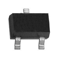
BSS138-7-F Diodes Zetex, BSS138-7-F Datasheet - Page 2

BSS138-7-F
Manufacturer Part Number
BSS138-7-F
Description
Manufacturer
Diodes Zetex
Type
Small Signalr
Datasheet
1.BSS138-7-F.pdf
(5 pages)
Specifications of BSS138-7-F
Number Of Elements
1
Polarity
N
Channel Mode
Enhancement
Drain-source On-res
3.5Ohm
Drain-source On-volt
50V
Gate-source Voltage (max)
±20V
Drain Current (max)
200mA
Output Power (max)
Not RequiredW
Frequency (max)
Not RequiredMHz
Noise Figure
Not RequireddB
Power Gain
Not RequireddB
Drain Efficiency
Not Required%
Operating Temp Range
-55C to 150C
Operating Temperature Classification
Military
Mounting
Surface Mount
Pin Count
3
Package Type
SOT-23
Power Dissipation
300mW
Lead Free Status / RoHS Status
Compliant
Available stocks
Company
Part Number
Manufacturer
Quantity
Price
Company:
Part Number:
BSS138-7-F
Manufacturer:
Diodes Inc
Quantity:
849 662
Company:
Part Number:
BSS138-7-F
Manufacturer:
Diodes
Quantity:
5 335
Part Number:
BSS138-7-F
Manufacturer:
DIODES/美台
Quantity:
20 000
Company:
Part Number:
BSS138-7-F-K-HN
Manufacturer:
DIODES
Quantity:
27 000
Thermal Characteristics
Electrical Characteristics
Maximum Ratings
Drain-Source Voltage
Drain-Gate Voltage R
Gate-Source Voltage
Drain Current
Power Dissipation (Note 4)
Thermal Resistance, Junction to Ambient (Note 4)
Operating and Storage Temperature Range
OFF CHARACTERISTICS (Note 5)
Drain-Source Breakdown Voltage
Zero Gate Voltage Drain Current
Gate-Body Leakage
ON CHARACTERISTICS (Note 5)
Gate Threshold Voltage
Static Drain-Source On-Resistance
Forward Transconductance
DYNAMIC CHARACTERISTICS
Input Capacitance
Output Capacitance
Reverse Transfer Capacitance
SWITCHING CHARACTERISTICS
Turn-On Delay Time
Turn-Off Delay Time
Notes:
BSS138
Document number: DS30144 Rev. 14 - 2
0.6
0.5
0.4
0.3
0.2
0.1
4. Device mounted on FR-5 PCB 1.0 x 0.75 x 0.062 inch pad layout as shown on Diodes, Inc. suggested pad layout AP02001, which can be found on our
5. Short duration pulse test used to minimize self-heating effect.
0
Fig. 1 Drain-Source Current vs. Drain-Source Voltage
0
website at http://www.diodes.com.
T = 25 C
j
1
V , DRAIN-SOURCE VOLTAGE (V)
GS
°
DS
2
≤ 20KΩ
Characteristic
Characteristic
Characteristic
3
@T
4
A
= 25°C unless otherwise specified
5
@T
@T
A
6
= 25°C unless otherwise specified
A
= 25°C unless otherwise specified
7
V
V
V
V
GS
GS
8
Continuous
GS
Continuous
GS
V
= 3.25V
GS
= 3.5V
= 2.75V
= 3.0V
= 2.5V
9
10
www.diodes.com
Symbol
R
BV
V
t
t
DS (ON)
D(OFF)
I
C
D(ON)
I
C
2 of 5
GS(th)
C
g
DSS
GSS
oss
FS
DSS
iss
rss
T
Symbol
Symbol
J
V
V
V
R
, T
P
DGR
GSS
DSS
I
θ JA
D
Min
100
D
0.5
50
STG
⎯
⎯
⎯
⎯
⎯
⎯
⎯
⎯
0.6
0.5
0.4
0.2
0.8
0.7
0.3
0.1
0
0
Typ
1.2
1.4
75
⎯
⎯
⎯
⎯
⎯
⎯
⎯
⎯
0.5
V
DS
V
±100
Max
GS
0.5
1.5
3.5
8.0
⎯
⎯
50
25
20
20
= 1V
Fig. 2 Transfer Characteristics
, GATE-SOURCE VOLTAGE (V)
1
-55 to +150
Unit
mS
µA
nA
pF
pF
pF
ns
ns
1.5
Ω
V
V
Value
Value
±20
200
300
417
50
50
V
V
V
V
V
V
V
V
GS
DS
GS
DS
GS
DS
DS
DD
2
= 50V, V
= V
= 25V, I
= 10V, V
= 30V, I
= 0V, I
= ±20V, V
= 10V, I
2.5
GS
, I
Test Condition
D
D
D
D
D
= 250μA
GS
GS
3
= 0.2A, f = 1.0KHz
= 0.2A, R
= 250μA
= 0.22A
DS
= 0V
= 0V, f = 1.0MHz
= 0V
3.5
-55 C °
© Diodes Incorporated
Units
Units
°C/W
mW
BSS138
mA
150 C °
°C
4
GEN
V
V
V
25 C °
January 2011
4.5
= 50Ω


