BSS8402DW-7-F Diodes Zetex, BSS8402DW-7-F Datasheet
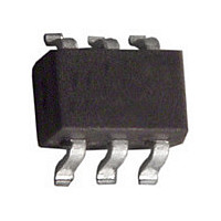
BSS8402DW-7-F

Manufacturer Part Number
BSS8402DW-7-F
Description
Manufacturer
Diodes Zetex
Type
Small Signalr
Datasheet

Specifications of BSS8402DW-7-F

Number Of Elements
2
Polarity
N/P
Channel Mode
Enhancement
Drain-source On-volt
60V
Gate-source Voltage (max)
±20V
Drain Current (max)
115mA
Output Power (max)
Not RequiredW
Frequency (max)
Not RequiredMHz
Noise Figure
Not RequireddB
Power Gain
Not RequireddB
Drain Efficiency
Not Required%
Operating Temp Range
-55C to 150C
Operating Temperature Classification
Military
Mounting
Surface Mount
Pin Count
6
Package Type
SOT-363
Power Dissipation
200mW
Lead Free Status / RoHS Status
Compliant

Available stocks

Company
Part Number
Manufacturer
Quantity
Price
Part Number:
BSS8402DW-7-F
Manufacturer:
DIODES
Quantity:
36 000
Part Number:
BSS8402DW-7-F
Manufacturer:
DIODES
Quantity:
27 000
Part Number:
BSS8402DW-7-F
Manufacturer:
DIODES
Quantity:
220
Part Number:
BSS8402DW-7-F
Manufacturer:
DIODES/美台
Quantity:
20 000
Part Number:
BSS8402DW-7-F
0
Company:
Part Number:
BSS8402DW-7-F
Quantity:
174 000
Part Number:
BSS8402DW-7-F-HN
Manufacturer:
DIODES
Quantity:
21 000
Maximum Ratings – Total Device
Maximum Ratings N-CHANNEL – Q
Maximum Ratings P-CHANNEL – Q
Power Dissipation (Note 1)
Thermal Resistance, Junction to Ambient
Operating and Storage Temperature Range
Drain-Source Voltage
Drain-Gate Voltage R
Gate-Source Voltage
Drain Current (Note 1)
Drain-Source Voltage
Drain-Gate Voltage R
Gate-Source Voltage
Drain Current (Note 1)
Features
Notes:
BSS8402DW
Document number: DS30380 Rev. 12 - 2
Low On-Resistance
Low Gate Threshold Voltage
Low Input Capacitance
Fast Switching Speed
Low Input/Output Leakage
Complementary Pair
Lead Free/RoHS Compliant (Note 2)
"Green" Device (Note 3 and 4)
Qualified to AEC-Q101 Standards for High Reliability
1. Device mounted on FR-4 PCB, 1 inch x 0.85 inch x 0.062 inch; pad layout as shown on Diodes Inc. suggested pad layout document AP02001, which
2. No purposefully added lead.
3. Diodes Inc.'s "Green" policy can be found on our website at http://www.diodes.com/products/lead_free/index.php.
4. Product manufactured with Date Code UO (week 40, 2007) and newer are built with Green Molding Compound. Product manufactured prior to Date
can be found on our website at http://www.diodes.com/datasheets/ap02001.pdf.
Code UO are built with Non-Green Molding Compound and may contain Halogens or Sb2O3 Fire Retardants.
GS
GS
≤ 1.0MΩ
≤ 20KΩ
Characteristic
Characteristic
Characteristic
COMPLEMENTARY PAIR ENHANCEMENT MODE FIELD EFFECT TRANSISTOR
Continuous @ 100°C
TOP VIEW
Continuous
Continuous
@T
Continuous
Continuous
2
1
, BSS84 Section
, 2N7002 Section
A
Pulsed
Pulsed
= 25°C unless otherwise specified
www.diodes.com
SOT-363
1 of 5
Mechanical Data
Symbol
T
Symbol
Symbol
J,
V
V
V
V
V
V
R
P
DGR
GSS
DGR
GSS
T
DSS
I
DSS
I
Please click here to visit our online spice models database.
θ JA
D
D
D
STG
Case: SOT-363
Case Material: Molded Plastic. “Green” Molding Compound.
UL Flammability Classification Rating 94V-0
Moisture Sensitivity: Level 1 per J-STD-020D
Terminals: Solderable per MIL-STD-202, Method 208
Lead Free Plating (Matte Tin Finish annealed over Alloy 42
leadframe).
Terminal Connections: See Diagram
Marking Information: See Page 5
Ordering Information: See Page 5
Weight: 0.008 grams (approximate)
Q
1
@T
@T
Internal Schematic
S
A
D
1
A
1
= 25°C unless otherwise specified
TOP VIEW
= 25°C unless otherwise specified
G
G
2
1
S
D
-55 to +150
2
2
Value
Value
Value
-130
200
625
±20
±40
115
800
±20
-50
-50
60
60
73
Q
2
BSS8402DW
© Diodes Incorporated
Units
Units
Units
°C/W
mW
mA
mA
°C
V
V
V
V
V
V
June 2008

Related parts for BSS8402DW-7-F

BSS8402DW-7-F Summary of contents

Page 1

... Symbol V DSS V DGR Continuous V GSS Pulsed Continuous Continuous @ 100° Pulsed , BSS84 Section @ Symbol V DSS V DGR Continuous V GSS Continuous www.diodes.com BSS8402DW TOP VIEW Value Units 200 mW 625 °C/W -55 to +150 °C = 25°C unless otherwise specified A Value Units ±20 V ±40 115 ...

Page 2

... GS(th) ⎯ ⎯ (ON) ⎯ ⎯ . ⎯ ⎯ iss ⎯ ⎯ oss ⎯ ⎯ rss ⎯ ⎯ D(ON) ⎯ ⎯ D(OFF www.diodes.com BSS8402DW @T = 25°C unless otherwise specified A Unit Test Condition ⎯ 0V 10μ 1 µ 60V ±20V 2 250μ 5.0V 0.05A 7.5 ...

Page 3

... V = 10V 200mA 120 145 0 ° 250 200 150 100 Fig. 6 Max Power Dissipation vs. Ambient Temperature www.diodes.com BSS8402DW ° 0.2 0.4 0.6 0 DRAIN CURRENT (A) D Fig. 2 On-Resistance vs. Drain Current GATE TO SOURCE VOLTAGE (V) GS Fig. 4 On-Resistance vs. Gate-Source Voltage 50 75 100 125 150 ...

Page 4

... Document number: DS30380 Rev -1.0 -0.8 -0.6 -0.4 -0.2 -0 ° 125 C A ° -10V GS -0.8 1 www.diodes.com BSS8402DW GATE-TO-SOURCE VOLTAGE (V) GS Fig. 8 Drain Current vs. Gate-Source Voltage V = -10V -0.13A D - 100 125 T , JUNCTION TEMPERATURE (°C) J Fig. 10 On-Resistance vs. Junction Temperature © Diodes Incorporated -7 -8 150 June 2008 ...

Page 5

... Ordering Information (Note 6) Part Number BSS8402DW-7-F Notes: 6. For packaging details our website at http://www.diodes.com/datasheets/ap02007.pdf. Marking Information Date Code Key Year 2003 2004 Code P R Month Jan Feb Code 1 2 Package Outline Dimensions Suggested Pad Layout Diodes Incorporated and its subsidiaries reserve the right to make modifications, enhancements, improvements, corrections or other changes without further notice to any product herein. Diodes Incorporated does not assume any liability arising out of the application or use of any product described herein ...

Related keywords