NUF2042XV6T1G ON Semiconductor, NUF2042XV6T1G Datasheet
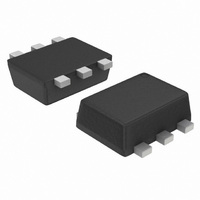
IC FILTER USB ESD PROTECT SOT363

NUF2042XV6T1G

Manufacturer Part Number
NUF2042XV6T1G
Description
IC FILTER USB ESD PROTECT SOT363
Manufacturer
ON Semiconductor
Datasheet

Specifications of NUF2042XV6T1G

Resistance (ohms)
22
Capacitance
42pF
Package / Case
SOT-563, SOT-6
Resistance In Ohms
22.0
Product
EMI Filters
Maximum Dc Current
100 nAmps
Maximum Dc Resistance
26.4 Ohms
Operating Temperature Range
- 55 C to + 125 C
Lead Free Status / RoHS Status
Lead free / RoHS Compliant
Power (watts)
-
Tolerance
-
Lead Free Status / Rohs Status
Lead free / RoHS Compliant
Other names
NUF2042XV6T1G
NUF2042XV6T1GOSTR

Available stocks

Company
Part Number
Manufacturer
Quantity
Price
Part Number:
NUF2042XV6T1G
Manufacturer:
ON
Quantity:
8 000
Part Number:
NUF2042XV6T1G
Manufacturer:
ON/安森美
Quantity:
20 000
Part Number:
NUF2042XV6T1G
Manufacturer:
ON
Quantity:
16 583
Part Number:
NUF2042XV6T1G
0
Company:
Part Number:
NUF2042XV6T1G
Quantity:
20 000
NUF2030XV6, NUF2042XV6
USB Upstream Terminator
with ESD Protection
Termination, EMI Filtering and ESD Protection. They are intended
for use in upstream USB ports, cellular phones, wireless equipment
and computer applications. These devices offer an integrated solution
in a small package (SOT−563) reducing PCB space and cost.
Features:
Benefits:
Typical Applications:
Maximum ratings are those values beyond which device damage can occur.
Maximum ratings applied to the device are individual stress limit values (not
normal operating conditions) and are not valid simultaneously. If these limits are
exceeded, device functional operation is not implied, damage may occur and
reliability may be affected.
© Semiconductor Components Industries, LLC, 2005
July, 2005 − Rev. 2
MAXIMUM RATINGS
Steady State Power
Maximum Junction Temperature
Operating Temperature Range
Storage Temperature Range
Lead Solder Temperature
(10 second duration)
These devices are designed for applications requiring Line
the System
:
Component Implementation
Implementation because the Small IC minimizes Parasitic
Inductances
Provides USB Line Termination, Filtering and ESD Protection
Single IC Offers Cost Savings
Bidirectional EMI Filtering Prevents Noise from Entering/Leaving
Compliance with IEC61000−4−2 (Level 4)
ESD Ratings: Machine Model = C
These are Pb−Free Devices
SOT−563 Package Minimizes PCB Space
Integrated Circuit Increases System Reliability versus Discrete
TVs Devices Provide ESD Protection That is Better than a Discrete
USB Hubs
Computer Peripherals Using USB
8 kV (Contact)
15 kV (Air)
Rating
Human Body Model = 3B
(T
A
= 25°C)
Symbol
T
J(max)
T
P
T
T
stg
D
J
L
−55 to +125
−55 to +125
Value
225
125
260
1
Unit
mW
°C
°C
°C
°C
See detailed ordering and shipping information in the package
dimensions section on page 5 of this data sheet.
xx = Specific Device Code
M
G
(Note: Microdot may be in either location)
R
S
D
= Month Code
= Pb−Free Package
ORDERING INFORMATION
D
1(0)
6
1
1(i)
CIRCUIT DESCRIPTION
(see table on page 5)
MARKING DIAGRAM
http://onsemi.com
C
1
CASE 463A
6
1
SOT−563
xx M G
V
GND
BUS
Publication Order Number:
5
2
G
1
C
1
NUF2030XV6/D
D
D
2(0)
4
3
2(i)
R
S

Related parts for NUF2042XV6T1G

NUF2042XV6T1G Summary of contents

Page 1

NUF2030XV6, NUF2042XV6 USB Upstream Terminator with ESD Protection These devices are designed for applications requiring Line Termination, EMI Filtering and ESD Protection. They are intended for use in upstream USB ports, cellular phones, wireless equipment and computer applications. These devices ...

Page 2

... ELECTRICAL CHARACTERISTICS V RWM (V) Min Device NUF2030XV6T1 5.25 5.6 NUF2042XV6T1 5.25 5.6 1. Measured between pins and ground with pin 5 also grounded. 2. For other resistance value (e.g. 33 W), please contact your local ON Semiconductor sales representative. NUF2030XV6, NUF2042XV6 (T = 25°C unless otherwise noted 3 (V) (nA) ...

Page 3

FREQUENCY (Hz) Figure 1. Insertion Loss Characteristics (NUF2030) 0 −5 −10 −15 −20 −25 −30 1.E+06 1.E+07 1.E+08 FREQUENCY (Hz) Figure 3. Insertion Loss Characteristics (NUF2042 ...

Page 4

NUF2030XV6, NUF2042XV6 24.5 24.0 23.5 23.0 22.5 22.0 21.5 −20 − TEMPERATURE (°C) Figure 7. R versus Temperature S (NUF2030 and NUF2042) http://onsemi.com Typical ...

Page 5

... Device Marking Device NUF2030XV6T1 30 NUF2030XV6T1G 30 NUF2042XV6T1 22 NUF2042XV6T1G 22 †For information on tape and reel specifications, including part orientation and tape sizes, please refer to our Tape and Reel Packaging Specifications Brochure, BRD8011/D. *These packages are inherently Pb−Free. NUF2030XV6, NUF2042XV6 Package SOT−563* SOT−563* SOT− ...

Page 6

... M *For additional information on our Pb−Free strategy and soldering details, please download the ON Semiconductor Soldering and Mounting Techniques Reference Manual, SOLDERRM/D. ON Semiconductor and are registered trademarks of Semiconductor Components Industries, LLC (SCILLC). SCILLC reserves the right to make changes without further notice to any products herein ...

Related keywords