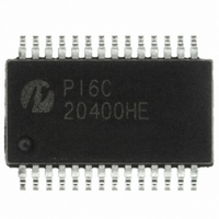
PI6C20400HE Pericom Semiconductor, PI6C20400HE Datasheet - Page 2

PI6C20400HE
Manufacturer Part Number
PI6C20400HE
Description
IC CLOCK BUFF DIFF 28-SSOP
Manufacturer
Pericom Semiconductor
Type
Clock Driverr
Datasheet
1.PI6C20400HE.pdf
(10 pages)
Specifications of PI6C20400HE
Input
HCSL
Output
HCSL
Frequency - Max
100MHz
Voltage - Supply
3.135 V ~ 3.465 V
Operating Temperature
0°C ~ 70°C
Mounting Type
Surface Mount
Package / Case
28-SSOP
Frequency-max
100MHz
Lead Free Status / RoHS Status
Lead free / RoHS Compliant
Available stocks
Company
Part Number
Manufacturer
Quantity
Price
Pin Descriptions
Serial Data Interface (SMBus)
PI6C20400 is a slave only SMBus device that supports indexed block read and indexed block write protocol using a single 7-bit
address and read/write bit as shown below.
Address assignment
Data Protocol
Notes:
1.
SRC & SRC#
OE_0 & OE_3
OE_INV
OUT[0:3] & OUT[0:3]#
PLL/BYPASS#
SCLK
SDA
IREF
SRC_STOP#
PLL_BW#
PWRDWN#
V
VSS
VSS_A
VDD_A
Start
1 bit
bit
DD
Register offset for indicating the starting register for indexed block write and indexed block read. Byte Count in write mode cannot be 0.
A6
1
08-0298
Pin Name
7 bits
Slave
Addr
R/W
A5
1
1
Input
Input
Input
Output
Input
Input
I/O
Input
Input
Input
Input
Power
Ground
Ground
Power
Ack
Type
1
Register
offset
8 bits
A4
0
2, 3
8, 21
25
6, 7, 9, 10, 19, 20,
22, 23
12
13
14
26
16
17
15
1, 5, 11, 18, 24
4
27
28
Pin No
Ack
1
A3
1
Count
8 bits
Byte
= N
0.7V Differential SRC input from PI6C410 clock synthesizer
3.3V LVTTL input for enabling outputs, active high.
OE_0 for OUT0 / OUT0#
OE_3 for OUT3 / OUT3#
3.3V LVTTL input for inverting the OE, SRC_STOP# and
PWRDWN# pins.
When 0 = same stage
When 1 = OE_0, OE_3, SRC_STOP#, PWRDWN# inverted.
0.7V Differential outputs
3.3V LVTTL input for selecting fan-out of PLL operation.
SMBus compatible SCLOCK input
SMBus compatible SDATA
External resistor connection to set the differential output current
3.3V LVTTL input for SRC stop, active low
3.3V LVTTL input for selecting the PLL bandwidth
3.3V LVTTL input for Power Down operation, active low
3.3V Power Supply for Outputs
Ground for Outputs
Ground for PLL
3.3V Power Supply for PLL
2
Ack
1
A2
1
Byte 0
8 bits
Data
A1
1
Ack
1
Description
…
1:4 Clock Driver for Intel
PCI Express Chipsets
A0
Byte N
0
8 bits
Data
- 1
PS8744C
Ack
1
PI6C20400
R/W
0/1
1 bit
Stop
bit
11/13/08


