ICS9248AG-92LFT IDT, Integrated Device Technology Inc, ICS9248AG-92LFT Datasheet
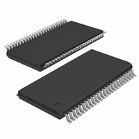
IC PENTIUM II CLOCK CHIP 48TSSOP

ICS9248AG-92LFT

Manufacturer Part Number
ICS9248AG-92LFT
Description
IC PENTIUM II CLOCK CHIP 48TSSOP
Manufacturer
IDT, Integrated Device Technology Inc
Type
Frequency Generatorr
Datasheet

Specifications of ICS9248AG-92LFT

Input
Crystal
Output
Clock
Frequency - Max
100MHz
Voltage - Supply
3.135 V ~ 3.465 V
Operating Temperature
0°C ~ 70°C
Mounting Type
Surface Mount
Package / Case
48-TSSOP
Frequency-max
100MHz
Lead Free Status / RoHS Status
Lead free / RoHS Compliant
Other names
9248AG-92LFT

Available stocks

Company
Part Number
Manufacturer
Quantity
Price
Part Number:
ICS9248AG-92LFT
Manufacturer:
ON
Quantity:
6 191
Block Diagram
General Description:
Features include two strong CPU, seven PCI and eight SDRAM
clocks. Three reference outputs are available equal to the
crystal frequency. Stronger drive CPUCLK outputs typically
provide greater than 1 V/ns slew rate into 20pF loads. This
device meets rise and fall requirements with 2 loads per CPU
output (ie, one clock to CPU and NB chipset, one clock to two
L2 cache inputs).
PWR_DWN# pin allows low power mode by stopping crystal
OSC and PLL stages. For optional power management,
CPU_STOP# can stop CPU (0:1) clocks and PCI_STOP# will
stop PCICLK (0:5) clocks
PCICLK outputs typically provide better than 1V/ns slew rate
into 30pF loads while maintaining 50±5% duty cycle. The REF
clock outputs typically provide better than 0.5V/ns slew rates.
The ICS9248-92 accepts a 14.318MHz reference crystal or
clock as its input and runs on a 3.3V core supply.
Pentium is a trademark on Intel Corporation.
Recommended Application:
The ICS9248-92 is a fully compliant timing solution for the
Intel mobile 440BX/MX chipset requirements.
Mobile Pentium II
9248-92 Rev E 02/21/01
Integrated
Circuit
Systems, Inc.
TM
System Clock Chip
Features
Functionality
Crystal (X1, X2) = 14.31818 MHz
1
Generates system clocks for CPU, SDRAM, PCI, plus
14.318 MHz REF(0:2), USB, Plus Super I/O
I
disabling and other functions
MODE input pin selects optional power management
input control pins
Two fixed outputs separately selectable as 24 or 48MHz
2.5V outputs: CPU
3.3V outputs: SDRAM, PCI, REF, 48/24 MHz
No power supply sequence requirements
Uses external 14.318MHz crystal
48 pin 240 mil TSSOP package
Output enable register
for serial port control:
0 0
S
2
48-Pin TSSOP 240 mil Package
C serial configuration interface provides output clock
E
0
6 /
1
L
ICS reserves the right to make changes in the device data identified in
this publication without further notice. ICS advises its customers to
obtain the latest version of all device data to verify that any
information being relied upon by the customer is current and accurate.
# 6
Pin Configuration
C
(
P
M
6 6
U
1
0 0
H
C
6 .
L
) z
K
1 = enable
0 = disable
P
ICS9248-92
C
(
M
3 3
3 3
I
C
H
3 .
3 .
L
) z
K

Related parts for ICS9248AG-92LFT

ICS9248AG-92LFT Summary of contents

Page 1

Integrated Circuit Systems, Inc. TM Mobile Pentium II Recommended Application: The ICS9248- fully compliant timing solution for the Intel mobile 440BX/MX chipset requirements. General Description: Features include two strong CPU, seven PCI and eight SDRAM clocks. Three reference ...

Page 2

Pin Descriptions ...

Page 3

Power-On Conditions ...

Page 4

General I The information in this section assumes familiarity with I For more information, contact ICS for an I How to Write: • Controller (host) sends a start bit. • Controller (host) sends the write address D2 • ICS clock ...

Page 5

Serial Configuration Command Bitmaps Byte 0: Functional and Frequency Select Clock Register (default on Bits Note: PWD = Power-Up Default ...

Page 6

Byte 1: CPU, 24/48 MHz Clock Register ...

Page 7

Power Management Clock Enable Configuration Full clock cycle timing ...

Page 8

CPU_STOP# Timing Diagram CPUSTOP asychronous input to the clock synthesizer used to turn off the CPUCLKs for low power operation. CPU_STOP# is synchronized by the ICS9248-92. The minimum that the CPUCLK is enabled (CPU_STOP# high pulse) ...

Page 9

Notes: 1. All timing is referenced to the Internal CPUCLK (defined as inside the ICS9248 device.) 2. PCI_STOP asynchronous input, and metastable conditions may exist. This signal is required to be synchronized inside the ICS9248. 3. All other ...

Page 10

Absolute Maximum Ratings Supply Voltage . . . . . . . . . . . . . . . . . . . . . . . . . . . 5.5 V Logic Inputs . . . . ...

Page 11

Electrical Characteristics - CPUCLK 70º 3.3 V +/-5 PARAMETER SYMBOL Period period(norm) V Output High Voltage V OH2B Output Low Voltage V OL2B Output High Current I OH2B Output Low ...

Page 12

Electrical Characteristics - PCICLK 70º 3.3 V +/-5 ETER SYM BOL Output High Voltage Output Low Voltage Output High ...

Page 13

General Layout Precautions: 1) Use a ground plane on the top routing layer of the PCB in all areas not used by traces. 2) Make all power traces and ground traces as wide as the via pad for lower inductance. ...

Page 14

Body, 0.50 mm. pitch TSSOP (0.020 mil) (240 mil) Ordering Information ICS9248yG-92 Example: ICS XXXX PPP Pattern Number ( digit number for parts with ROM code patterns) Package Type G=TSSOP Revision Designator Device ...

Related keywords