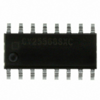
CY25568SXC Cypress Semiconductor Corp, CY25568SXC Datasheet - Page 4

CY25568SXC
Manufacturer Part Number
CY25568SXC
Description
IC CLOCK GEN 3.3V SS 16-SOIC
Manufacturer
Cypress Semiconductor Corp
Type
Clock/Frequency Synthesizer, Fanout Distribution, Frequency Modulator, Spread Spectrum Clock Generatorr
Datasheet
1.CY25568SXC.pdf
(11 pages)
Specifications of CY25568SXC
Number Of Circuits
1
Package / Case
16-SOIC (3.9mm Width)
Pll
Yes
Input
Clock, Crystal, Resonator
Output
Clock
Ratio - Input:output
1:4
Differential - Input:output
No/No
Frequency - Max
128MHz
Divider/multiplier
Yes/Yes
Voltage - Supply
2.9 V ~ 3.6 V
Operating Temperature
0°C ~ 70°C
Mounting Type
Surface Mount
Frequency-max
128MHz
Maximum Input Frequency
32 MHz
Minimum Input Frequency
4 MHz
Output Frequency Range
4 MHz to 128 MHz
Supply Voltage (max)
3.6 V
Supply Voltage (min)
2.9 V
Maximum Operating Temperature
+ 70 C
Minimum Operating Temperature
0 C
Mounting Style
SMD/SMT
Operating Supply Voltage
3.3 V
Lead Free Status / RoHS Status
Lead free / RoHS Compliant
Lead Free Status / RoHS Status
Lead free / RoHS Compliant, Lead free / RoHS Compliant
Other names
428-2224-5
CY25568SXC
CY25568SXC
Available stocks
Company
Part Number
Manufacturer
Quantity
Price
Company:
Part Number:
CY25568SXC
Manufacturer:
Cypress Semiconductor Corp
Quantity:
1 924
Company:
Part Number:
CY25568SXC
Manufacturer:
SMSC
Quantity:
473
Part Number:
CY25568SXC
Manufacturer:
CYPRESS/赛普拉斯
Quantity:
20 000
Input Frequency Range and Selection
The CY25568 input frequency range is 4 to 32 MHz. This range is divided into 3 segments and controlled by 3-Level FRSEL pin as
given in
Table 1. Input Frequency Selection
Output Clocks
The CY25568 provides 4 separate output clocks, REFOUT, SSCLK1, SSCLK2 and SSCLK3, for use in a wide variety of applications.
Each clock output is described in detail.
REFOUT
REFOUT is a 3.3-volt CMOS level non-modulated copy of the clock at XIN/CLKIN.
SSCLK1, 2 and 3
SSCLK1, SSCLK2 and SSCLK3 are Spread Spectrum clock outputs used for the purpose of reducing EMI in digital systems. Each
clock can drive separate nets with a capacitive load of up to 20 pF.
The frequency function of these clock outputs are selected by using 3-Level D0 and D1 digital inputs and are given in
Table 2. Output Clocks Function Selection
REF is the same non-modulated frequency as the input clock.
1x, 2x, or 4x are modulated and multiplied (in the case of 2x and 4x) frequency of the input clock.
Document Number: 38-07111 Rev. *C
D0
M
M
M
FRSEL
0
0
0
1
1
1
M
Table
0
1
1.
D1
M
M
M
0
1
0
1
0
1
INPUT FREQUENCY RANGE
16.0 to 32.0 MHz
8.0 to 16.0 MHz
4.0 to 8.0 MHz
REFOUT
REF
REF
REF
REF
REF
REF
REF
REF
REF
SSCLK1
REF
REF
REF
REF
REF
REF
1x
1x
1x
SSCLK2
REF
1x
2x
2x
1x
2x
4x
2x
2x
SSCLK3
CY25568
REF
Table
1x
2x
2x
2x
4x
4x
4x
4x
Page 4 of 11
2.
[+] Feedback


