CY29972AXI Cypress Semiconductor Corp, CY29972AXI Datasheet
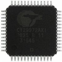
IC CLK ZDB 12OUT 125MHZ 52TQFP

CY29972AXI

Manufacturer Part Number
CY29972AXI
Description
IC CLK ZDB 12OUT 125MHZ 52TQFP
Manufacturer
Cypress Semiconductor Corp
Type
Fanout Distribution, Multiplexer , Spread Spectrum Clock Generator, Zero Delay Bufferr
Datasheet

Specifications of CY29972AXI

Number Of Circuits
1
Package / Case
52-TQFP
Pll
Yes with Bypass
Input
Clock, Crystal
Output
Clock
Ratio - Input:output
4:12
Differential - Input:output
No/No
Frequency - Max
125MHz
Divider/multiplier
Yes/No
Voltage - Supply
2.9 V ~ 3.6 V
Operating Temperature
-40°C ~ 85°C
Mounting Type
Surface Mount
Frequency-max
125MHz
Maximum Input Frequency
480 MHz
Minimum Input Frequency
200 MHz
Output Frequency Range
125 MHz
Supply Voltage (max)
3.6 V
Supply Voltage (min)
2.9 V
Maximum Operating Temperature
+ 85 C
Minimum Operating Temperature
- 40 C
Mounting Style
SMD/SMT
Operating Supply Voltage
3.3 V
Lead Free Status / RoHS Status
Lead free / RoHS Compliant
Lead Free Status / RoHS Status
Lead free / RoHS Compliant, Lead free / RoHS Compliant
Other names
428-2236
CY29972AXI

Available stocks

Company
Part Number
Manufacturer
Quantity
Price
Part Number:
CY29972AXI
Manufacturer:
CY
Quantity:
4 918
Part Number:
CY29972AXI
Manufacturer:
Cypress Semiconductor Corp
Quantity:
10 000
Part Number:
CY29972AXIT
Manufacturer:
Cypress Semiconductor Corp
Quantity:
10 000
Part Number:
CY29972AXIT
Manufacturer:
CYPRESS
Quantity:
20 000
Cypress Semiconductor Corporation
Document #: 38-07290 Rev. *C
Features
• Output frequency up to 125 MHz
• 12 Clock outputs: frequency configurable
• 350 ps max. output-to-output skew
• Configurable output disable
• Two reference clock inputs for dynamic toggling
• Oscillator or crystal reference input
• Spread-spectrum-compatible
• Glitch-free output clocks transitioning
• 3.3V power supply
• Pin-compatible with MPC972
• Industrial temperature range: –40°C to +85°C
• 52-pin TQFP package
Block Diagram
FB_SEL(0,1)
TCLK_SEL
SELC(0,1)
VCO_SEL
SELA(0,1)
SELB(0,1)
REF_SEL
FB_SEL2
INV_CLK
MR#/OE
PLL_EN
SDATA
TCLK0
TCLK1
XOUT
FB_IN
SCLK
XIN
Power-On
Reset
0
1
2
2
2
2
Detector
Phase
Output Disable
Data Generator
Circuitry
/4, /6, /8, /12
/4, /6, /8, /10
/4, /6, /8, /10
/2, /4, /6, /8
Sync Pulse
LPF
VCO
12
3.3V, 125-MHz Multi-Output Zero Delay Buffer
0
1
/2
0
1
D Q
D Q
D Q
D Q
D Q
D Q
3901 North First Street
Sync
Sync
Sync
Sync
Sync
Sync
Frz
Frz
Frz
Frz
Frz
Frz
QA0
QA1
QA2
QA3
QB0
QB1
QB2
QB3
QC0
QC1
QC2
QC3
FB_OUT
SYNC
Table 1. Frequency Table
Note:
VC0_SEL FB_SEL2 FB_SEL1 FB_SEL0
1. x = the reference input frequency, 200 MHz < F
TCLK_SEL
Pin Configuration
REF_SEL
FB_SEL2
MR#/OE
0
0
0
0
0
0
0
0
1
1
1
1
1
1
1
1
PLL_EN
SDATA
TCLK0
TCLK1
XOUT
SCLK
VDD
VSS
XIN
1
2
3
4
5
6
7
8
9
10
11
12
13
San Jose
52 51 50 49 48 47 46 45 44 43 42 41 40
14 15 16 17 18 19 20 21 22 23 24 25 26
0
0
0
0
1
1
1
1
0
0
0
0
1
1
1
1
CY29972
,
CA 95134
[1]
0
0
1
1
0
0
1
1
0
0
1
1
0
0
1
1
Revised October 28, 2005
VCO
0
1
0
1
0
1
0
1
0
1
0
1
0
1
0
1
< 480 MHz.
39
38
37
36
35
34
33
32
31
30
29
28
27
408-943-2600
CY29972
VSS
QB0
VDDC
QB1
VSS
QB2
VDDC
QB3
FB_IN
VSS
FB_OUT
VDDC
FB_SEL0
F
12x
16x
20x
16x
24x
32x
40x
10x
12x
16x
20x
VC0
8x
4x
6x
8x
8x
[+] Feedback

Related parts for CY29972AXI

CY29972AXI Summary of contents

Page 1

... LPF TCLK_SEL FB_IN FB_SEL2 MR#/OE Power-On Reset /4, /6, /8, /12 /4, /6, /8, /10 2 SELA(0,1) /2, /4, / SELB(0,1) 0 /4, /6, /8, / SELC(0,1) Sync Pulse 2 FB_SEL(0,1) Data Generator SCLK Output Disable 12 Circuitry SDATA INV_CLK Cypress Semiconductor Corporation Document #: 38-07290 Rev. *C Table 1. Frequency Table VC0_SEL FB_SEL2 FB_SEL1 FB_SEL0 ...

Page 2

Pin Description Pin Name PWR OUT 9 T CLK0 10 T CLK1 44, 46, 48, 50 QA(3:0) V DDC 32, 34, 36, 38 QB(3:0) V DDC 16, 18, 21, 23 QC(3:0) V DDC 29 ...

Page 3

Description The CY29972 has an integrated PLL that provides low skew and low jitter clock outputs for high-performance micropro- cessors. Three independent banks of four outputs and an independent PLL feedback output (FB_OUT) provide excep- tional flexibility for possible output ...

Page 4

SYNC Output In situations where output frequency relationships are not integer multiples of each other, the SYNC output provides a signal for system synchronization. The CY29972 monitors the relationship between the QA and QC output clocks. It provides a LOW-going ...

Page 5

Power Management The individual output enable/freeze control of the CY29972 allows the user to implement unique power management schemes into the design. The outputs are stopped in the logic ‘0’ state when the freeze control bits are activated. The serial ...

Page 6

... Part Number CY29972AI CY29972AIT Lead-free CY29972AXI CY29972AXIT Notes: 6. Inputs have pull-up/pull-down resistors that effect input current. 7. Driving series or parallel terminated 50Ω (or 50Ω Parameters are guaranteed by design and characterization. Not 100% tested in production. 9. Maximum and minimum input reference is limited by VC0 lock range. ...

Page 7

... Document #: 38-07290 Rev. *C © Cypress Semiconductor Corporation, 2005. The information contained herein is subject to change without notice. Cypress Semiconductor Corporation assumes no responsibility for the use of any circuitry other than circuitry embodied in a Cypress product. Nor does it convey or imply any license under patent or other rights. Cypress products are not warranted nor intended to be used for medical, life support, life saving, critical control or safety applications, unless pursuant to an express written agreement with Cypress ...

Page 8

Document History Page Document Title: CY29972 3.3V, 125-MHz Multi-Output Zero Delay Buffer Document Number: 38-07290 Issue REV. ECN NO. Date ** 111101 02/07/02 *A 122882 12/22/02 *B 387764 See ECN *C 404340 See ECN Document #: 38-07290 Rev. *C Orig. ...

Related keywords