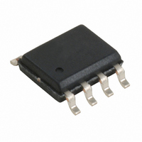
CY2304SXC-2 Cypress Semiconductor Corp, CY2304SXC-2 Datasheet - Page 8

CY2304SXC-2
Manufacturer Part Number
CY2304SXC-2
Description
IC CLK ZDB 4OUT 133MHZ 8SOIC
Manufacturer
Cypress Semiconductor Corp
Type
Fanout Distribution, Zero Delay Bufferr
Datasheet
1.CY2304SXC-2.pdf
(15 pages)
Specifications of CY2304SXC-2
Number Of Circuits
1
Package / Case
8-SOIC (3.9mm Width)
Pll
Yes
Input
Clock
Output
Clock
Ratio - Input:output
1:4
Differential - Input:output
No/No
Frequency - Max
133.3MHz
Divider/multiplier
Yes/Yes
Voltage - Supply
3 V ~ 3.6 V
Operating Temperature
0°C ~ 70°C
Mounting Type
Surface Mount
Frequency-max
133MHz
Output Frequency Range
10 MHz to 133.3 MHz
Supply Voltage (max)
3.6 V
Supply Voltage (min)
3 V
Maximum Operating Temperature
+ 70 C
Minimum Operating Temperature
0 C
Mounting Style
SMD/SMT
Operating Supply Voltage
3.3 V
Clock Ic Type
Clock Buffer
Frequency
133.33MHz
No. Of Outputs
4
No. Of Multipliers / Dividers
1
Supply Current
45mA
Supply Voltage Range
3V To 3.6V
Digital Ic Case Style
SOIC
No. Of Pins
8
Rohs Compliant
Yes
Lead Free Status / RoHS Status
Lead free / RoHS Compliant
Lead Free Status / RoHS Status
Lead free / RoHS Compliant, Lead free / RoHS Compliant
Other names
428-2894-5
CY2304SXC-2
CY2304SXC-2
Document Number: 38-07247 Rev. *J
Notes
Switching Characteristics for CY2304SXI Industrial Temperature Devices
t
t
t
t
t
t
t
t
t
t
t
t
t
t
t
8. All parameters are specified with loaded output.
9. Parameter is guaranteed by design and characterization. Not 100% tested in production.
1
1
DC
DC
DC
3
3
4
4
5
6
7
J
J
LOCK
Parameter
[8]
Output frequency
Output frequency
Duty cycle
(–1,–2)
Duty cycle
(–2)
Duty cycle
(–1,–2)
Rise time
(–1, –2)
Rise time
(–1, –2)
Fall time
(–1, –2)
Fall time
(–1, –2)
Output-to-output skew on
same bank (–1,–2)
Output bank A to output
bank B skew (–1)
Output bank A to output
bank B skew (–2)
Skew, REF rising edge to
FBK rising edge
Device-to-device skew
Cycle-to-cycle jitter
(–1)
Cycle-to-cycle jitter
(–2)
PLL lock time
[9]
[9]
[9]
[9]
[9]
[9]
[9]
Name
= t
= t
= t
[9]
2
2
2
[9]
t
t
t
[9]
[9]
[9]
1
1
1
[9]
30-pF load, All devices
15-pF load, All devices
Measured at 1.4 V, F
30-pF load
Measured at 1.4 V,
F
Measured at 1.4 V, F
15-pF load
Measured between 0.8 V and 2.0 V,
30-pF load
Measured between 0.8 V and 2.0 V,
15-pF load
Measured between 0.8 V and 2.0 V,
30-pF load
Measured between 0.8 V and 2.0 V,
15-pF load
All outputs equally loaded
All outputs equally loaded
All outputs equally loaded
Measured at V
Measured at V
devices
Measured at 66.67 MHz, loaded outputs,
15-pF load
Measured at 66.67 MHz, loaded outputs,
30-pF load
Measured at 133.3 MHz, loaded outputs,
15-pF load
Measured at 66.67 MHz, loaded outputs,
30-pF load
Measured at 66.67 MHz, loaded outputs,
15-pF load
Stable power supply, valid clocks
presented on REF and FBK pins
OUT
= 83.0 MHz, 15-pF load
Test Conditions
DD
DD
/2
/2 on the FBK pins of
OUT
OUT
= 66.66 MHz,
< 50 MHz,
40.0
40.0
45.0
Min
10
10
–
–
–
–
–
–
–
–
–
–
–
–
–
–
–
50.0
50.0
50.0
Typ
–
–
–
–
–
–
–
–
–
0
0
–
–
–
–
–
–
133.3
250
Max
60.0
60.0
55.0
2.50
1.50
2.50
1.50
100
200
200
400
500
180
200
100
400
380
1.0
CY2304
Page 8 of 15
MHz
MHz
Unit
ms
ns
ns
ns
ns
ps
ps
ps
ps
ps
ps
ps
ps
ps
ps
%
%
%
[+] Feedback


