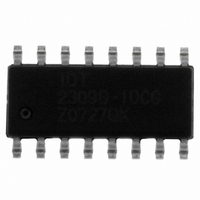
IDT2309B-1DCG IDT, Integrated Device Technology Inc, IDT2309B-1DCG Datasheet

IDT2309B-1DCG
Specifications of IDT2309B-1DCG
800-1299
800-1299-5
800-1299
Related parts for IDT2309B-1DCG
IDT2309B-1DCG Summary of contents
Page 1
... REF pin. The PLL feedback is on-chip and is obtained from the CLKOUT pad. In the absence of an input clock, the IDT2309B enters power down, and the outputs are tri-stated. In this mode, the device will draw less than 25μA. The IDT2309B is characterized for both Industrial and Commercial operation ...
Page 2
... IDT2309B 3.3V ZERO DELAY CLOCK BUFFER PIN CONFIGURATION REF 1 2 CLKA1 CLKA2 GND 6 CLKB1 CLKB2 SOIC/ TSSOP TOP VIEW APPLICATIONS: • SDRAM • Telecom • Datacom • PC Motherboards/Workstations • Critical Path Delay Designs PIN DESCRIPTION Pin Name Pin Number REF 1 (1) ...
Page 3
... OUT Measured between 0.8V and 2V Measured between 0.8V and 2V All outputs equally loaded Measured (2) DD Measured PLL bypass mode (IDT2309B only) (2) DD Measured the CLKOUT pins of devices DD Measured at 66.66MHz, loaded outputs Stable power supply, valid clock presented on REF pin 3 CLKOUT ...
Page 4
... IDT2309B 3.3V ZERO DELAY CLOCK BUFFER SWITCHING CHARACTERISTICS (2309B-1H) - COMMERCIAL Symbol Parameter t Output Frequency 1 ÷ t Duty Cycle = Duty Cycle = t ÷ Rise Time 3 t Fall Time 4 t Output to Output Skew 5 t Delay, REF Rising Edge to CLKOUT Rising Edge 6A t Delay, REF Rising Edge to CLKOUT Rising Edge ...
Page 5
... Measured between 0.8V and 2V Measured between 0.8V and 2V All outputs equally loaded Measured Measured PLL bypass mode (IDT2309B only) DD Measured the CLKOUT pins of devices DD Measured between 0.8V and 2V using Test Circuit 2 Measured at 66.66MHz, loaded outputs Stable power supply, valid clock presented on REF pin ...
Page 6
... IDT2309B 3.3V ZERO DELAY CLOCK BUFFER ZERO DELAY AND SKEW CONTROL All outputs should be uniformly loaded in order to achieve Zero I/O Delay. Since the CLKOUT pin is the internal feedback for the PLL, its relative loading can affect and adjust the input/output delay. The Output Load Difference diagram illustrates the PLL's relative loading with respect to the other outputs that can adjust the Input-Output (I/O) Delay ...
Page 7
... IDT2309B 3.3V ZERO DELAY CLOCK BUFFER SWITCHING WAVEFORMS t1 t2 1.4V 1.4V Duty Cycle Timing 2V 0.8V 0.8V 2V Output t3 All Outputs Rise/Fall Time TEST CIRCUITS V DD 0.1 F OUTPUTS V DD 0.1 F GND GND Test Circuit 1 (all Parameters Except t8) COMMERCIAL AND INDUSTRIAL TEMPERATURE RANGES Output 1 ...
Page 8
... Number of Loaded Outputs NOTES: 1. Duty Cycle is taken from typical chip measured at 1.4V data is calculated from nCVf, where CORE V = Supply Voltage (V Frequency (Hz)) COMMERCIAL AND INDUSTRIAL TEMPERATURE RANGES AND I TRENDS FOR IDT2309B-1 (1) ( 33MHz 50 66MHz 100MHz 3.5 3 -40C ...
Page 9
... Number of Loaded Outputs NOTES: 1. Duty Cycle is taken from typical chip measured at 1.4V data is calculated from IDD = ICORE + nCVf, where ICORE is the unloaded current Number of outputs Capacitance load per output (F Supply Voltage (V Frequency (Hz)) COMMERCIAL AND INDUSTRIAL TEMPERATURE RANGES AND I TRENDS FOR IDT2309B-1H (1) ( 33MHz ...
Page 10
... IDT2309B 3.3V ZERO DELAY CLOCK BUFFER ORDERING INFORMATION XXXXX XX X IDT Package Process Device Type Ordering Code IDT2309B-1DCG IDT2309B-1DCGI IDT2309B-1HDCG IDT2309B-1HDCGI IDT2309B-1HPGGI IDT2309B-1HPGG CORPORATE HEADQUARTERS 6024 Silver Creek Valley Road San Jose, CA 95138 COMMERCIAL AND INDUSTRIAL TEMPERATURE RANGES Blank Commercial (0 I Industrial (-40 ...


