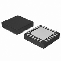
NB4N441MNG ON Semiconductor, NB4N441MNG Datasheet

NB4N441MNG
Specifications of NB4N441MNG
Available stocks
Related parts for NB4N441MNG
NB4N441MNG Summary of contents
Page 1
... OSC SDATA SCLOCK SLOAD *For additional information on our Pb−Free strategy and soldering details, please download the ON Semiconductor Soldering and Mounting Techniques Reference Manual, SOLDERRM/D. © Semiconductor Components Industries, LLC, 2007 February, 2007 − Rev. 1 *For additional marking information, refer to Application Note AND8002/D. ...
Page 2
V LOCKED CC Input Prescaler CLK/XTAL1 XTAL PB R OSC XTAL2 FB SDATA SCLOCK Frequency Control Logic SLOAD GND 24 1 GND VCC_PLL GND 7 Figure 3. QFN−24 Lead Pinout (Top View) ...
Page 3
Table 1. PIN DESCRIPTION Pin Name 11, 12, 13 VCC_PLL 18, 19 GND 20 LOCKED 10 CLK / XTAL1, LVTTL/LVCMOS Single Ended 7 XTAL2 15 SLOAD** 16 ...
Page 4
Table 2. STANDARD PROTOCOL / OUTPUT FREQUENCY SELECT TABLE WITH 27 MHz CRYSTAL REFERENCE # Protocol 0 OC−3 /STM−1 0 OC−12 / STM−4 0 OC−48 / STM−16 1 ETR 2 OC−1 3 Fast Ethernet 3 ESCON 4 FDDI 4 Infiniband ...
Page 5
Table 4. ATTRIBUTES Internal Input Pullup Resistor Internal Input Pulldown Resistor ESD Protection Moisture Sensitivity (Note 1) Flammability Rating Transistor Count Meets or exceeds JEDEC Spec EIA/JESD78 IC Latchup Test 1. For additional information, see Application Note AND8003/D. Table 5. ...
Page 6
Table 6. DC CHARACTERISTICS V CC Symbol Characteristic I Power Supply Current (Inputs and Outputs Loaded PLL Power Supply Current CCPLL V LVPECL Output HIGH Voltage (Notes 4 and LVPECL Output LOW Voltage (Notes 4 ...
Page 7
General The NB4N441 is a precision clock synthesizer which generates a differential LVPECL clock output frequency from 12.5 MHz to 425 MHz. A three−wire SPI interface is used to configure the device to produce the exact frequency of one of ...
Page 8
PLL_V 0. 0.01 mF Figure 4. Power Supply Filter Power Supply Filtering The NB4N441 is a mixed analog/digital product and as such, it exhibits ...
Page 9
S_CLOCK S_DATA First S_LOAD S_DATA S_CLOCK S_DATA S_LOAD NB4N441 Bit Figure 5. Serial Interface Timing Diagram t HOLD t SETUP Figure 6. Setup and Hold t HOLD t SETUP Figure 7. Setup ...
Page 10
Jitter Performance Jitter is a common parameter associated with clock generation and distribution. Clock jitter can be defined as the deviation in a clock’s output transition from its ideal position. Cycle−to−Cycle Jitter (short−term) is the period variation between two adjacent ...
Page 11
... Figure 10. Typical Termination for Output Driver and Device Evaluation (See Application Note AND8020/D − Termination of ECL Logic Devices.) ORDERING INFORMATION Device NB4N441MNG NB4N441MNR2G †For information on tape and reel specifications, including part orientation and tape sizes, please refer to our Tape and Reel Packaging Specifications Brochure, BRD8011/D. ...
Page 12
... Opportunity/Affirmative Action Employer. This literature is subject to all applicable copyright laws and is not for resale in any manner. PUBLICATION ORDERING INFORMATION LITERATURE FULFILLMENT: Literature Distribution Center for ON Semiconductor P.O. Box 5163, Denver, Colorado 80217 USA Phone: 303−675−2175 or 800−344−3860 Toll Free USA/Canada Fax: 303− ...


