NJM567D NJR, NJM567D Datasheet
NJM567D
Specifications of NJM567D
Available stocks


Related parts for NJM567D


NJM567D Summary of contents
Page 1
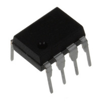
... Frequency adjustment over range with an external resistor ● Package Outline ● Bipolar Technology ■ PIN CONFIGURATION ■ BLOCK DIAGRAM Ver.2003-12-09 (4.75V to 9.0V) (0.01Hz to 500kHz) ( percent) DIP8, DMP8 PIN FUNCTION 1 OUTPUT FILTER 2 LOW-PASS FILTER 3 INPUT + TIMING R 6 TIMING CR 7 GROUND NJM567D 8 OUTPUT NJM567M ■ PACKAGE OUTLINE NJM567D NJM567M - 1 - ...
Page 2
ABSOLUTE MAXIMUM RATINGS PARAMETER SYMBOL Supply Voltage Input Positive Voltage Input Negative Voltage Output Voltage Power Dissipation Operating Temperature Range Storage Temperature Range ■ ELECTRICAL CHARACTERISTICS PARAMETER Highest Center Frequency Center Frequency Stability Center Frequency Shift with Supply Voltage ...
Page 3
TYPICAL CHARACTERISTICS Frequency Drift Ambient Temperatur Frequency Drift Center Frequency Shift Ver.2003-12-09 ° Frequency Drift Center Frequency Temperature = ° ~ ° Coefficient ∆ Detection Bandwidth - 3 - ...
Page 4
TYPICAL CHARACTERISTICS Bandwidth Detection Bandwidth vs. C Greatest Number of Cycles - 4 - Largest Detection Bandwidth , Operating Current Output Voltage Ver.2003-12-09 ...
Page 5
DESIGN FORMULAS 1.07R − BW 1070 where V : Input Voltage ...
Page 6
Output Terminal(Fig.2) The primary output is the uncommitted output transistor collector, pin 8. When an in-band input signal is present, this transistor saturates; its collector voltage being less than 1.0volt (typically 0.6V) at full output current (100mA). The voltage ...
Page 7
Speed of Operation Minimum lock-up time is related to the natural frequency of the loop. The lower it is, the longer becomes the turn-on transient. Thus, maximum operating speed is obtained when C phase may be such as to ...
Page 8
Chatter Prevention (Figure 4) Chatter occurs in the output stage when C quadrature phase detector (lock detector) output cause the output stage to move through its threshold more than once. Many loads, for example lamps and relays, will not ...
Page 9
Alternate Method of Bandwidth Reduction (Figure 6) Although a large value of C will reduce the bandwidth, it also reduces the loop damping slow the circuit 2 response time. This may be undesirable. Bandwidth can be ...
Page 10
Reduction of C Value (Figure 8) 1 For precision very low-frequency applictions, where the value of C achieved by inserting a voltage follower between the R lower value of C for a given frequency. 1 ◎ Programming To change ...