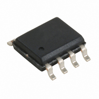
W180-01G Cypress Semiconductor Corp, W180-01G Datasheet

W180-01G
Specifications of W180-01G
Available stocks
Related parts for W180-01G
W180-01G Summary of contents
Page 1
... MHz Pin Configurations CLKIN Spread Spectrum Output (EMI suppressed) CLKIN Spread Spectrum Output (EMI suppressed) • 3901 North First Street • San Jose W180 W180-01, 02, 03 W180-51, 52, 53 Output Output – 0.625 out in in 1.25% 0.625 – 1.875% in out in in 3.75% – ...
Page 2
... Modulation Width Selection: When Spread Spectrum feature is turned on, this pin is used to select the amount of variation and peak EMI reduction that is desired on the output signal. Internal pull-up resistor. P Power Connection: Connected to 3. power supply. G Ground Connection: This should be connected to the common ground plane. Pin Description W180 Page ...
Page 3
... Overview The W180 products are one series of devices in the Cypress PREMIS family. The PREMIS family incorporates the latest advances in PLL spread spectrum frequency synthesizer tech- niques. By frequency modulating the output with a low-fre- quency carrier, peak EMI is greatly reduced. Use of this tech- nology allows systems to pass increasingly difficult EMI testing without resorting to costly shielding or redesign ...
Page 4
... Cypress spreading pattern. Cypress does offer options with more spread and greater EMI reduction. Contact your local Sales representative for details on these devices. Typical Clock Spread Spectrum Enabled Figure 3. Typical Modulation Profile W180 EMI Reduction Non- Spread Spectrum Frequency Span (MHz) Down Spread Page ...
Page 5
... Description : 0°C < T < 70° 3.3V ± Test Condition First locked clock cycle after Power Good Note 2 Note 2 @ 0.4V 3. 2.4V 3.3V DD W180 Rating Unit –0.5 to +7.0 V –65 to +150 ° +70 °C –55 to +125 °C 0.5 W Min. Typ. Max. Unit 18 ...
Page 6
... Spread Off, Note 4 15-pF load 0.8V–2.4V 15-pF load 2.4 –0.8V 15-pF load MHz, third harmonic out measured, reference board, 15-pF load Min. Typ. Max 0.15V DD 0.7V DD 0.4 2.4 – 500 25 Min. Typ. Max 250 300 8 Page W180 Unit Unit. MHz MHz ...
Page 7
... Plastic SOIC (150-mil) connection can be DD Clock Output C1 0.1 µ µF Tantalum High frequency supply decoupling C1 = capacitor (0.1- µF recommended Common supply low frequency decoupling capacitor (10- µF tantalum recommended Match value to line impedance FB = Ferrite Bead G = Via To GND Plane C1 G Clock Output R1 W180 Page ...
Page 8
... The inclusion of Cypress Semiconductor products in life-support systems application implies that the manufacturer assumes all risk of such use and in doing so indemnifies Cypress Semiconductor against all charges. W180 Page ...
Page 9
... Document Title: W180 Peak Reducing EMI Solution Document Number: 38-07156 Issue REV. ECN NO. Date ** 110266 12/15/01 *A 122588 12/27/02 Document #: 38-07156 Rev. *A Orig. of Change SZV Change from Spec number: 38-00796 to 38-07156 RBI Added power up requirements to maximum ratings information. Description of Change W180 Page ...


