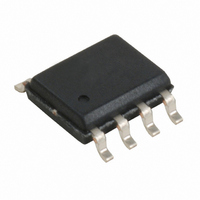
W181-02G Cypress Semiconductor Corp, W181-02G Datasheet - Page 6

W181-02G
Manufacturer Part Number
W181-02G
Description
CLOCK EMI REDUCTION SSCG 8-SOIC
Manufacturer
Cypress Semiconductor Corp
Series
Premis™r
Type
Clock/Frequency Synthesizer, Spread Spectrum Clock Generatorr
Datasheet
1.W181-01G.pdf
(9 pages)
Specifications of W181-02G
Pll
Yes
Input
Clock, Crystal
Output
CMOS
Number Of Circuits
1
Ratio - Input:output
1:1
Differential - Input:output
No/No
Frequency - Max
75MHz
Divider/multiplier
Yes/No
Voltage - Supply
3.135 V ~ 5.5 V
Operating Temperature
0°C ~ 70°C
Mounting Type
Surface Mount
Package / Case
8-SOIC (3.9mm Width)
Frequency-max
75MHz
Lead Free Status / RoHS Status
Contains lead / RoHS non-compliant
Other names
428-1396
Available stocks
Company
Part Number
Manufacturer
Quantity
Price
Company:
Part Number:
W181-02G
Manufacturer:
HARRIS
Quantity:
2 965
Company:
Part Number:
W181-02GI
Manufacturer:
HARRIS
Quantity:
18 683
Document #: 38-07152 Rev. *D
AC Electrical Characteristics:
CLKOUT Frequency Offset (Shift)
Application Information
Recommended Circuit Configuration
For optimum performance in system applications the power
supply decoupling scheme shown in Figure 4 should be used.
V
EMI radiation. The 0.1-µF decoupling capacitor should be
placed as close to the V
Notes:
f
f
t
t
t
t
t
FOFFSET-1
FOFFSET-2
FOFFSET-3
FOFFSET-4
4. The frequency offset (shift) is given with respect to ideal peak value which is the same as input reference frequency in the case of down spread only for W180-01,-02
5. There is no offset (shift) for center spread for W180-51,-52 and -53 products.
IN
OUT
R
F
OD
ID
JCYC
DD
and -03 products.
Parameter
Parameter
decoupling is important to both reduce phase jitter and
Frequency Offset (Shift)
Frequency Offset (Shift)
Frequency Offset (Shift)
Frequency Offset (Shift)
Input Frequency
Output Frequency
Output Rise Time
Output Fall Time
Output Duty Cycle
Input Duty Cycle
Jitter, Cycle-to-Cycle
Harmonic Reduction
Reference Input
Description
DD
Description
pin as possible, otherwise the
GND
NC
3.3 or 5V System Supply
Figure 4. Recommended Circuit Configuration
T
A
[4,5]
1
2
3
4
= 0°C to +70°C, V
:
T
Input Clock
Spread Off
V
V
15-pF load
f
measured, reference board,
15-pF load
out
A
DD
DD
= 0°C to +70°C, V
= 40 MHz, third harmonic
, 15-pF load 0.8V–2.4V
, 15-pF load 2.4V–0.8V
FS2=0, FS1=0, 28≤F
FS2=0, FS1=1, 38≤F
FS2=1, FS1=0, 46≤F
FS2=1, FS1=1, 58≤F
Frequency Range (MHz)
Test Condition
8
7
6
5
DD
R1
= 3.3V ±5% or 5V±10%
DD
increased trace inductance will negate its decoupling
capability. The 10-µF decoupling capacitor shown should be a
tantalum type. For further EMI protection, the V
can be made via a ferrite bead, as shown.
Recommended Board Layout
Figure 5 shows a recommended 2-layer board layout.
= 3.3V ±5% or 5V±10% (For only W181-02, -02 and -03 products)
FB
IN
IN
IN
IN
≤38
≤48
≤60
≤75
Clock
Output
Min.
28
28
40
40
8
Min.
–0.8
–1.1
–0.2
–0.8
C2
10-µF Tantalum
C1
0.1 µF
Typ.
250
2
2
Typ.
–1.0
–1.4
–0.5
–1.0
Max.
300
75
75
60
60
5
5
Max.
–1.2
–1.7
–0.8
–1.2
DD
Page 6 of 9
connection
W181
MHz
Unit
MHz
dB
ns
ns
ps
%
%
Unit
%
%
%
%


