CY28346ZXC Cypress Semiconductor Corp, CY28346ZXC Datasheet - Page 4
CY28346ZXC
Manufacturer Part Number
CY28346ZXC
Description
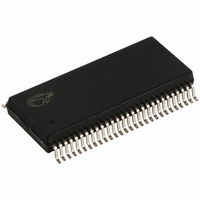
IC CLOCK SYNTHESIZER 56-TSSOP
Manufacturer
Cypress Semiconductor Corp
Type
Clock Synchronizer, Fanout Distribution, Spread Spectrum Clock Generatorr
Datasheet
1.CY28346OXC.pdf
(20 pages)
Specifications of CY28346ZXC
Pll
Yes
Input
Clock, Crystal
Output
Clock
Number Of Circuits
1
Ratio - Input:output
5:17
Differential - Input:output
No/Yes
Frequency - Max
200MHz
Divider/multiplier
Yes/No
Voltage - Supply
3.135 V ~ 3.465 V
Operating Temperature
0°C ~ 70°C
Mounting Type
Surface Mount
Package / Case
56-TSSOP II
Frequency-max
200MHz
Lead Free Status / RoHS Status
Lead free / RoHS Compliant
Available stocks
Company
Part Number
Manufacturer
Quantity
Price
Company:

Part Number:
CY28346ZXC-2
Manufacturer:
CY
Quantity:
63
Part Number:
CY28346ZXC-2
Manufacturer:
CYPRESS/赛普拉斯
Quantity:
20 000
Company:
Part Number:
CY28346ZXC2T
Manufacturer:
CYPR
Quantity:
2 611
Part Number:
CY28346ZXCT
Manufacturer:
CYPRESS/赛普拉斯
Quantity:
20 000


Document #: 38-07331 Rev. *C
Byte 2: PCI Clock Control Register (all bits are Read and Write functional)
Byte 3: PCI_F Clock and 48M Control Register (all bits are Read and Write functional)
Byte 4: DRCG Control Register (all bits are Read and Write functional)
Byte 5: Clock Control Register (all bits are Read and Write functional)
Bit
Bit
Bit
7
6
5
4
3
2
1
0
7
6
5
4
3
2
1
0
7
6
5
4
3
2
1
0
Bit
7
6
5
4
3
2
1
0
@Pup
@Pup
@Pup
0
1
0
0
0
0
0
0
0
0
1
1
1
1
1
1
@Pup
1
1
0
0
0
1
1
1
0
1
1
1
1
1
1
1
Pin#
Pin#
33
35
24
23
22
21
Pin#
38
39
7
6
5
7
6
5
Pin#
SS1 Spread Spectrum Control Bit.
SS0 Spread Spectrum Control Bit.
66IN to 66M delay Control MSB.
66IN to 66M delay Control LSB.
Reserved. Set = 0.
48MDOT Edge Rate Control. When set to 1, the edge is slowed by 15%.
Reserved. Set = 0.
USB edge rate control. When set to 1, the edge is slowed by 15%.
53
18
17
16
13
12
11
10
SS2 Spread Spectrum Control Bit (0 = down spread, 1 = center spread).
Reserved. Set = 0.
3V66_0 Output Enabled. 1 = enabled, 0 = disable.
3V66_1/VCH Output Enable. 1 = enabled, 0 = disabled.
3V66_5 Output Enable. 1 = enabled, 0 = disabled.
66B2/3V66_4 Output Enabled. 1 = enabled, 0 = disabled.
66B1/3V66_3 Output Enabled. 1 = enabled, 0 = disabled.
66B0/3V66_2 Output Enabled. 1 = enabled, 0 = disabled.
48MDOT Output Control. 1 = enabled, 0 = forced LOW.
48MUSB Output Control. 1 = enabled, 0 = forced LOW.
PCI_STP#, Control of PCI_F2. 0 = Free Running, 1 = Stopped when PCI_STP# is LOW.
PCI_STP#, Control of PCI_F1. 0 = Free Running, 1 = Stopped when PCI_STP# is LOW.
PCI_STP#, Control of PCI_F0. 0 = Free Running, 1 = Stopped when PCI_STP# is LOW.
PCI_F2 Output Control. 1 = running, 0 = forced LOW.
PCI_F1 Output Control. 1 = running, 0 = forced LOW.
PCI_F0 Output Control. 1 = running, 0 = forced LOW.
REF Output Control. 0 = high strength, 1 = low strength.
PCI6 Output Control. 1 = enabled, 0 = forced LOW.
PCI5 Output Control. 1 = enabled, 0 = forced LOW.
PCI4 Output Control. 1 = enabled, 0 = forced LOW.
PCI3 Output Control. 1 = enabled, 0 = forced LOW.
PCI2 Output Control. 1 = enabled, 0 = forced LOW.
PCI1 Output Control. 1 = enabled, 0 = forced LOW.
PCI0 Output Control. 1 = enabled, 0 = forced LOW.
Description
Description
Description
Description
CY28346
Page 4 of 20
Related parts for CY28346ZXC
Image
Part Number
Description
Manufacturer
Datasheet
Request
R

Part Number:
Description:
Manufacturer:
Cypress Semiconductor Corp
Datasheet:
Part Number:
Description:
Manufacturer:
Cypress Semiconductor Corp
Datasheet:
Part Number:
Description:
Manufacturer:
Cypress Semiconductor Corp
Datasheet:
Part Number:
Description:
Manufacturer:
Cypress Semiconductor Corp
Datasheet:
Part Number:
Description:
Manufacturer:
Cypress Semiconductor Corp
Datasheet: