CY28346ZXCT Cypress Semiconductor Corp, CY28346ZXCT Datasheet - Page 11
CY28346ZXCT
Manufacturer Part Number
CY28346ZXCT
Description
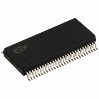
IC CLOCK SYNTHESIZER 56-TSSOP
Manufacturer
Cypress Semiconductor Corp
Type
Clock Synchronizer, Fanout Distribution, Spread Spectrum Clock Generatorr
Datasheet
1.CY28346OXC.pdf
(20 pages)
Specifications of CY28346ZXCT
Pll
Yes
Input
Clock, Crystal
Output
Clock
Number Of Circuits
1
Ratio - Input:output
5:17
Differential - Input:output
No/Yes
Frequency - Max
200MHz
Divider/multiplier
Yes/No
Voltage - Supply
3.135 V ~ 3.465 V
Operating Temperature
0°C ~ 70°C
Mounting Type
Surface Mount
Package / Case
56-TSSOP II
Frequency-max
200MHz
Lead Free Status / RoHS Status
Lead free / RoHS Compliant
Available stocks
Company
Part Number
Manufacturer
Quantity
Price

Part Number:
CY28346ZXCT
Manufacturer:
CYPRESS/赛普拉斯
Quantity:
20 000


Document #: 38-07331 Rev. *C
PCI_STP# – Deassertion (transition from logic “0”
to logic “1”)
The deassertion of the PCI_STP# signal will cause all PCI(0:6)
and stoppable PCI_F(0:2) clocks to resume running in a
synchronous manner within two PCI clock periods after
PCI_STP# transitions to a HIGH level.
Note. The PCI STOP function is controlled by two inputs. One
is the device PCI_STP# pin number 34 and the other is SMBus
Byte 0,Bit 3. These two inputs to the function are logically
AND’ed. If either the external pin or the internal SMBus
register bit is set LOW, the stoppable PCI clocks will be
stopped in a logic LOW state. Reading SMBus Byte 0,Bit 3 will
return a 0 value if either of these control bits are set LOW
(which indicates that the devices stoppable PCI clocks are not
running).
PD# (Power-down) Clarification
The PD# (power-down) pin is used to shut off all clocks prior
to shutting off power to the device. PD# is an asynchronous
active LOW input. This signal is synchronized internally to the
device powering down the clock synthesizer. PD# is an
PCI_F(0:2) 33M
PCI(0:6) 33M
PCI_F(0:2)
PCI_STP#
PCI_STP#
PCI(0:6)
Figure 12. PCI_STP# Deassertion Waveform
Figure 11. PCI_STP# Assertion Waveform
t
t
setup
setup
asynchronous function for powering up the system. When PD#
is LOW, all clocks are driven to a LOW value and held there
and the VCO and PLLs are also powered down. All clocks are
shut down in a synchronous manner so has not to cause
glitches while transitioning to the LOW “stopped” state.
PD# – Assertion
When PD# is sampled LOW by two consecutive rising edges
of the CPUC clock, then on the next HIGH-to-LOW transition
of PCIF, the PCIF clock is stopped LOW. On the next
HIGH-to-LOW transition of 66Buff, the 66Buff clock is stopped
LOW. From this time, each clock will stop LOW on its next
HIGH-to-LOW transition, except the CPUT clock. The CPU
clocks are held with the CPUT clock pin driven HIGH with a
value of 2 × Iref, and CPUC undriven. After the last clock has
stopped, the rest of the generator will be shut down.
PD# – Deassertion
The power-up latency between PD# rising to a valid logic ‘1’
level and the starting of all clocks is less than 3.0 ms.
CY28346
Page 11 of 20
Related parts for CY28346ZXCT
Image
Part Number
Description
Manufacturer
Datasheet
Request
R

Part Number:
Description:
Manufacturer:
Cypress Semiconductor Corp
Datasheet:
Part Number:
Description:
Manufacturer:
Cypress Semiconductor Corp
Datasheet:
Part Number:
Description:
Manufacturer:
Cypress Semiconductor Corp
Datasheet:
Part Number:
Description:
Manufacturer:
Cypress Semiconductor Corp
Datasheet:
Part Number:
Description:
Manufacturer:
Cypress Semiconductor Corp
Datasheet: