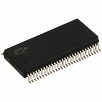
CY28RS400ZXCT Cypress Semiconductor Corp, CY28RS400ZXCT Datasheet

CY28RS400ZXCT
Specifications of CY28RS400ZXCT
Related parts for CY28RS400ZXCT
CY28RS400ZXCT Summary of contents
Page 1
... IREF PD PLL2 2 SDATA I C SCLK Logic Cypress Semiconductor Corporation Document #: 38-07637 Rev. *B Clock Generator for ATI • Low-voltage frequency select input 2 • support with readback capabilities • Ideal Lexmark Spread Spectrum profile for maximum electromagnetic interference (EMI) reduction • 3.3V power supply • ...
Page 2
Pin Description Pin No. Name Type 47,46,43,42, CPUT/C[2:0] O, DIF Differential CPU clock output. 41,40 50 PCI0/409_410 I/ IREF I 54 REF0/ FSA I/O, SE, 14.318MHz REF clock ouput/ CPU Frequency Select. Intel 53 REF1/FSB I/O, SE 14.318MHz ...
Page 3
Frequency Select Pins (FS_A, FS_B, FS_C and 409_410) Host clock frequency selection is achieved by applying the appropriate logic levels to FS_A, FS_B, FS_C and 409_410 inputs prior to VTT_PWRGD# assertion (as seen by the clock synthesizer). Upon VTT_PWRGD# being ...
Page 4
Table 4. Block Read and Block Write Protocol (continued) Block Write Protocol Bit Description 27:20 Byte Count – 8 bits 28 Acknowledge from slave 36:29 Data byte 1 – 8 bits 37 Acknowledge from slave 45:38 Data byte 2 – ...
Page 5
Control Registers Byte 0:Control Register 0 Bit @Pup Name 7 1 SRC[T/C SRC[T/C SRC[T/C SRC[T/C SRC[T/C SRC [T/C SRCS[T/C SRCS[T/C]0 Byte 1: Control Register 1 Bit ...
Page 6
Byte 2: Control Register 2 (continued) Bit @Pup Name 0 1 Reserved Byte 3: Control Register 3 Bit @Pup Name 7 1 CLKREQ CPU 5 1 SRC 4 0 CPU 3 1 CPU2 2 1 CPU1 1 1 ...
Page 7
Byte 5: Control Register 5 (continued) Bit @Pup Name 5 0 SRC[T/C SRC[T/C SRC[T/C SRC[T/C Reserved 0 0 Reserved Byte 6: Control Register 6 Bit @Pup Name 7 0 TEST_SEL 6 0 ...
Page 8
Crystal Recommendations The CY28RS400 requires a Parallel Resonance Crystal. Substituting a series resonance crystal will cause the CY28RS400 to operate at the wrong frequency and violate the ppm specification. For most applications there is a 300-ppm frequency shift between series ...
Page 9
As mentioned previously, the capacitance on each side of the crystal is in series with the crystal. This mean the total capac- itance on each side of the crystal must be twice the specified load capacitance (CL). While the capacitance ...
Page 10
PD CPUT, 133MHz CPUC, 133MHz SRCT 100MHz SRCC 100MHz USB, 48MHz DOT96T DOT96C PCI, 33MHz REF Figure 4. Power-down Deassertion Timing Waveform CPU_STP# Assertion The CPU_STP# signal is an active low input used for synchronous stopping and starting the CPU ...
Page 11
CPU_STOP# PD CPUT(Free Running CPUC(Free Running CPUT(Stoppable) CPUC(Stoppable) Figure 7. CPU_STP#= Driven, CPU_PD = Driven CPU_STOP# PD CPUT(Free Running) CPUC(Free Running) CPUT(Stoppable) CPUC(Stoppable) CLK_REQ[0:1]# Description The CLKREQ#[1:0] signals are active low input used for clean stopping and starting selected SRC ...
Page 12
FS_A, FS_B,FS_C VTT_PW RGD# PW RGD_VRM 0.2-0.3mS VDD Clock Gen Clock State State 0 Off Clock Outputs Off Clock VCO VDD_A = 2.0V S0 Power Off Figure 11. Clock Generator Power-up/Run State Diagram Document #: 38-07637 Rev ait ...
Page 13
Absolute Maximum Conditions Parameter Description V Core Supply Voltage DD V Analog Supply Voltage DDA V Input Voltage IN T Temperature, Storage S T Temperature, Operating Ambient A T Temperature, Junction J ESD ESD Protection (Human Body Model) HBM Ø ...
Page 14
AC Electrical Specifications (continued) Parameter Description T XIN Period PERIOD XIN Rise and Fall Times XIN Cycle to Cycle Jitter CCJ L Long-term Accuracy ACC CPU at 0.7V T CPUT and CPUC Duty Cycle ...
Page 15
AC Electrical Specifications (continued) Parameter Description T 100-MHz SRCT and SRCC Period, SSC PERIODSS T 100-MHz SRCT and SRCC Absolute Period PERIODAbs T 100-MHz SRCT and SRCC Absolute Period, SSC Measured at crossing point V PERI- ODSSAbs T Any SRCT/C ...
Page 16
AC Electrical Specifications (continued) Parameter Description REF Rise and Fall Times REF Cycle to Cycle Jitter CCJ ENABLE/DISABLE and SET-UP T Clock Stabilization from Power-up STABLE T Stopclock Set-up Time SS T Stopclock Hold ...
Page 17
... CY28RS400ZCT 56-pin TSSOP – Tape and Reel Lead-free CY28RS400OXC 56-pin SSOP CY28RS400OXCT 56-pin SSOP – Tape and Reel CY28RS400ZXC 56-pin TSSOP CY28RS400ZXCT 56-pin TSSOP – Tape and Reel Package Diagrams 56-Lead Shrunk Small Outline Package O56 28 29 0.720 0.730 0.088 0.092 ...
Page 18
... Document #: 38-07637 Rev. *B © Cypress Semiconductor Corporation, 2004. The information contained herein is subject to change without notice. Cypress Semiconductor Corporation assumes no responsibility for the use of any circuitry other than circuitry embodied in a Cypress product. Nor does it convey or imply any license under patent or other rights. Cypress products are not warranted nor intended to be used for medical, life support, life saving, critical control or safety applications, unless pursuant to an express written agreement with Cypress ...
Page 19
Document History Page Document Title: CY28RS400 Clock Generator for ATI Document Number: 38-07637 REV. ECN NO. Issue Date ** 204582 See ECN *A 215824 See ECN *B 278494 See ECN Document #: 38-07637 Rev. *B RS400 Chipset Orig. of ...


