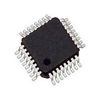
IDT5V9885BPFGI IDT, Integrated Device Technology Inc, IDT5V9885BPFGI Datasheet - Page 4

IDT5V9885BPFGI
Manufacturer Part Number
IDT5V9885BPFGI
Description
IC CLK GEN 3.3V EEPROM 32-TQFP
Manufacturer
IDT, Integrated Device Technology Inc
Type
Clock Generatorr
Datasheet
1.IDT5V9885BNLGI.pdf
(37 pages)
Specifications of IDT5V9885BPFGI
Pll
Yes with Bypass
Input
LVCMOS, LVTTL, Crystal
Output
LVCMOS, LVDS, LVPECL, LVTTL
Number Of Circuits
1
Ratio - Input:output
2:8
Differential - Input:output
No/Yes
Frequency - Max
500MHz
Divider/multiplier
Yes/Yes
Voltage - Supply
3.135 V ~ 3.6 V
Operating Temperature
-40°C ~ 85°C
Mounting Type
Surface Mount
Package / Case
32-TQFP, 32-VQFP
Frequency-max
500MHz
Number Of Elements
3
Supply Current
120mA
Pll Input Freq (min)
1MHz
Pll Input Freq (max)
400MHz
Operating Supply Voltage (typ)
3.3V
Operating Temp Range
-40C to 85C
Package Type
TQFP
Output Frequency Range
0.0049 to 500MHz
Operating Supply Voltage (min)
3V
Operating Supply Voltage (max)
3.6V
Operating Temperature Classification
Industrial
Pin Count
32
Lead Free Status / RoHS Status
Lead free / RoHS Compliant
Other names
5V9885BPFGI
Available stocks
Company
Part Number
Manufacturer
Quantity
Price
Company:
Part Number:
IDT5V9885BPFGI
Manufacturer:
IDT, Integrated Device Technology Inc
Quantity:
10 000
Part Number:
IDT5V9885BPFGI
Manufacturer:
IDT
Quantity:
20 000
Company:
Part Number:
IDT5V9885BPFGI8
Manufacturer:
IDT, Integrated Device Technology Inc
Quantity:
10 000
PIN DESCRIPTION
NOTES:
1. The JTAG (TDO, TMS, TCLK, TRST, and TDI) and I
2. Weak internal 100KΩ pull-down resistor.
3. 3-level inputs are static inputs and must be tied to V
4. Outputs are user programmable to drive single-ended 3.3V LVTTL, differential LVDS, or differential LVPECL interface levels.
IDT5V9885B
3.3V EEPROM PROGRAMMABLE CLOCK GENERATOR
GOUT0/TDO/LOSS_LOCK
GOUT1/LOSS_CLKIN
GIN1/SCLK/TCK
GIN3/SUSPEND
SHUTDOWN/OE
GIN0/SDAT/TDI
GIN5/CLK_SEL
XTALIN/REFIN
GIN4/TRST
GIN2/TMS
Pin Name
XTALOUT
I
2
CLKIN
C/JTAG
OUT1
OUT2
OUT3
OUT4
OUT4
OUT5
OUT5
OUT6
GND
V
DD
23,26,32
7,12,17,
2,9,14,
PF32
18,30
Pin#
19
20
24
27
25
21
28
22
29
10
11
15
16
13
31
1
4
5
6
8
3
10,15,20
2,12,26
NL28
Pin#
16
17
21
23
22
18
24
19
25
13
14
11
27
28
1
4
5
6
7
8
9
3
DD
2
C (SCLK and SDAT) signals share the same pins with GIN signals.
or GND or left floating. These inputs are internally biased to V
I/O
O
O
O
O
O
O
O
O
O
O
O
I
I
I
I
I
I
I
I
I
I
Adjustable
Adjustable
Adjustable
Adjustable
LVTTL
LVTTL
LVTTL
LVTTL
LVTTL
LVTTL
LVTTL
3-level
LVTTL
LVTTL
LVTTL
LVTTL
LVTTL
LVTTL
LVTTL
LVTTL
LVTTL
Type
(1,2)
(1,2)
(1,2)
(1,2)
(1,2)
(1,2)
(1,2)
(3)
(1)
(4)
(4)
(4)
(4)
4
Description
Input Clock
CRYSTAL_IN - Reference crystal input or external reference clock input
CRYSTAL_OUT -Reference crystal feedback
Multi-purpose inputs. Can be used for Frequency Control, SDAT(I
Multi-Purpose inputs. Can be used for Frequency Control, SCLK(I
Multi-Purpose inputs. Can be used for Frequency Control or TMS (JTAG)
Multi-Purpose inputs. Can be used for Frequency Control or as a suspend mode control
input (active HIGH).
Multi-Purpose inputs. Can be used for Frequency Control or TRST (JTAG)
Multi-Purpose inputs. Can be used for Frequency Control or input clock selector.
Enables/disables the outputs or powers down the chip. The SP bit (0x1C) controls the
polarity of the signal to be either active HIGH or LOW. (Default is active HIGH.)
I
Configurable clock output 1. Can also be used to buffer the reference clock.
Configurable clock output 2
Configurable clock output 3
Configurable clock output 4, Single-Ended or Differential when combined with OUT4
Configurable complementary clock output 4, Single-Ended or Differential when
combined with OUT4
Configurable clock output 5, Single-Ended or Differential when combined with OUT5
Configurable complementary clock output 5, Single-Ended or Differential when
combined with OUT5
Configurable clock output 6
Multi-Purpose Output. Can be programmed to use as PLL LOCK signal, LOSS_LOCK
or TDO in JTAG mode
Multi-Purpose Output. Can be programmed to use as LOSS_CLKIN
3.3V Power Supply
Ground
2
C (HIGH) or MFC Mode (MID) or JTAG Programming (LOW)
DD
/2. They are not hot-insertable or over voltage tolerant.
INDUSTRIAL TEMPERATURE RANGE
2
2
C), or TCK(JTAG).
C), or TDI(JTAG).


