SI4133-BT Silicon Laboratories Inc, SI4133-BT Datasheet
SI4133-BT
Specifications of SI4133-BT
Available stocks


Related parts for SI4133-BT


SI4133-BT Summary of contents
Page 1
... N RFOUT RFLC RFLD RF2 ÷ N IFDIV IFOUT IF IFLA ÷ N IFLB Copyright © 2003 by Silicon Laboratories Si4133 Si4123/22/13/ Ordering Information: See page 31. Pin Assignments Si4133- SCLK SEN 2 23 SDATA VDDI 3 22 GNDR IFOUT 4 21 RFLD GNDI 5 20 RFLC IFLB 6 19 GNDR ...
Page 2
... Si4133 2 Rev. 1.4 ...
Page 3
... PLL Loop Dynamics . . . . . . . . . . . . . . . . . . . . . . . . . . . . . . . . . . . . . . . . . . . . . . . . . . 18 RF and IF Outputs . . . . . . . . . . . . . . . . . . . . . . . . . . . . . . . . . . . . . . . . . . . . . . . . . . . 19 Reference Frequency Amplifier . . . . . . . . . . . . . . . . . . . . . . . . . . . . . . . . . . . . . . . . . 19 Powerdown Modes . . . . . . . . . . . . . . . . . . . . . . . . . . . . . . . . . . . . . . . . . . . . . . . . . . . 19 Auxiliary Output (AUXOUT Control Registers . . . . . . . . . . . . . . . . . . . . . . . . . . . . . . . . . . . . . . . . . . . . . . . . . . . . . . . 21 Pin Descriptions: Si4133- Pin Descriptions: Si4133- Ordering Guide . . . . . . . . . . . . . . . . . . . . . . . . . . . . . . . . . . . . . . . . . . . . . . . . . . . . . . . . . 31 Si4133 Derivative Devices . . . . . . . . . . . . . . . . . . . . . . . . . . . . . . . . . . . . . . . . . . . . . . . . 31 Package Outline: Si4133- Package Outline: Si4133- Document Change List . . . . . . . . . . . . . . . . . . . . . . . . . . . . . . . . . . . . . . . . . . . . . . . . . . 34 Contact Information . . . . . . . . . . . . . . . . . . . . . . . . . . . . . . . . . . . . . . . . . . . . . . . . . . . . . 36 Rev. 1.4 Si4133 Page 3 ...
Page 4
... Si4133 Electrical Specifications Table 1. Recommended Operating Conditions Parameter Ambient Temperature Supply Voltage Supply Voltages Difference Note: All minimum and maximum specifications are guaranteed and apply across the recommended operating conditions. Typical values apply at nominal supply voltages and an operating temperature of 25 °C unless otherwise stated. ...
Page 5
... For signals SCLK, SDATA, SEN, and PWDN. 3. For signal AUXOUT. Symbol Test Condition RF1 and IF operating PWDN = –500 µ 500 µ Rev. 1.4 Si4133 Min Typ Max Unit — — — — — 1 — µA 0.7 V — — — — 0 –10 — 10 µA –10 — ...
Page 6
... Si4133 Table 4. Serial Interface Timing (V = 2 – ° Parameter SCLK Cycle Time SCLK Rise Time SCLK Fall Time SCLK High Time SCLK Low Time 2 SDATA Setup Time to SCLK↑ 2 SDATA Hold Time from SCLK↑ 2 SEN↓ to SCLK↑ Delay Time 2 SCLK↑ ...
Page 7
... S CLK D17 t en1 Figure 2. Serial Interface Timing Diagram First bit c loc ked hold D16 D15 data field Figure 3. Serial Word Format Rev. 1.4 Si4133 en3 t en2 t w Last bit clocked address field 7 ...
Page 8
... Extended frequency operation only. V RFLB pins. See Application Note 41 for more details on the Si4133 extended frequency operation. 3. From powerup request (PWDN↑ or SEN↑ during a write bits PDIB and PDRB in Register and IF synthesizers ready (settled to within 0.1 ppm frequency error). ...
Page 9
... Extended frequency operation only. V RFLB pins. See Application Note 41 for more details on the Si4133 extended frequency operation. 3. From powerup request (PWDN↑ or SEN↑ during a write bits PDIB and PDRB in Register and IF synthesizers ready (settled to within 0.1 ppm frequency error). ...
Page 10
... Si4133 SDATA Figure 4. Software Power Management Timing Diagram PWDN Figure 5. Hardware Power Management Timing Diagram 10 RF and IF synthesizers settled to within 0.1 ppm frequency error. t pup PWDN SEN PDIB = 1 PDIB = 0 PDRB = 1 PDRB = 0 RF and IF synthesizers settled to within 0.1 ppm frequency error. t pup ...
Page 11
... TRACE A: Ch1 FM Main Time A Marker 1.424 kHz Real 160 Hz /div 176 Hz Start Figure 6. Typical Transient Response RF1 at 1.6 GHz with 200 kHz Phase Detector Update Frequency Rev. 1.4 us 174.04471 711.00 Stop: 399.6003996 us Si4133 Hz 11 ...
Page 12
... Si4133 −60 −70 −80 −90 −100 −110 −120 −130 −140 2 10 Figure 7. Typical RF1 Phase Noise at 1.6 GHz with 200 kHz Phase Detector Update Frequency Figure 8. Typical RF1 Spurious Response at 1.6 GHz with 200 kHz Phase Detector Update Frequency Offset Frequency (Hz) Rev ...
Page 13
... Offset Frequency (Hz) Figure 9. Typical RF2 Phase Noise at 1.2 GHz with 200 kHz Phase Detector Update Frequency Figure 10. Typical RF2 Spurious Response at 1.2 GHz with 200 kHz Phase Detector Update Frequency Rev. 1 Si4133 13 ...
Page 14
... Si4133 −70 −80 −90 −100 −110 −120 −130 −140 −150 2 10 Figure 11. Typical IF Phase Noise at 550 MHz with 200 kHz Phase Detector Update Frequency Figure 12. IF Spurious Response at 550 MHz with 200 kHz Phase Detector Update Frequency Offset Frequency (Hz) Rev. 1.4 ...
Page 15
... RFLC 6 19 IFLA GNDR 7 18 RFLB GNDD VDDD RFLA 9 16 GNDR GNDD 10 15 GNDR XIN 11 14 PWDN RFOUT µ VDDR AUXOUT Figure 13. Si4133- Ω * 0.022 µ GNDR GNDI 20 RFLD IFLB 19 RFLC IFLA 18 Si4133-BM GNDR GNDD 17 RFLB VDDD 16 RFLA GNDD 15 GNDR XIN ...
Page 16
... MHz and as high as 952 MHz output divider divides down the IF output frequencies, if needed. The divider is programmable and is capable of dividing The unique PLL architecture used in the Si4133 produces settling (lock) times that are comparable in speed to fractional-N architectures without the high phase noise or spurious modulation effects often for RF associated with those designs ...
Page 17
... Figure 15. External Inductance Connection As a design example, consider that the goal is to synthesize frequencies MHz band between 1120 and 1145 MHz using the Si4133-BT. The center frequency should be defined as midway between the two extremes, or 1132.5 MHz. The PLL can adjust the VCO output frequency ± ...
Page 18
... The settling time for the PLL is directly proportional to its phase detector update period T φ (T φ equals 1/f φ typical transient response is shown in Figure 6 on page 11. During the first 13 update periods the Si4133 Only the executes the self-tuning algorithm. From then on the PLL controls the output frequency ...
Page 19
... PWDN pin is high, power management is in control of the 27 nH Powerdown register bits The IF and RF sections of the Si4133 circuitry can be individually powered down by setting the Powerdown register bits PDIB and PDRB low, respectively. The reference frequency amplifier is also powered up if the PDRB and PDIB bits are high. Also, setting the AUTOPDB ...
Page 20
... Si4133 Auxiliary Output (AUXOUT) The signal appearing on AUXOUT is selected by setting the AUXSEL bits in the Main Configuration register (Register 0). The LDETB signal can be selected by setting the AUXSEL bits to 11. This signal can be used to indicate that the PLL is going to lose lock because of excessive ambient temperature drift and should be re-tuned. The LDETB signal indicates a logical OR result if both IF and RF are simultaneously generating a signal ...
Page 21
... Bit Bit Bit Bit Bit Bit Bit Bit AUXSEL IFDIV [1:0] [1: [17:0] RF1 N [16:0] RF2 Rev. 1.4 Si4133 Bit Bit Bit Bit Bit Bit LPWR AUTO AUTO RF PDB K PWR [1:0] [1: PDIB [15:0] R [12:0] RF1 R [12:0] RF2 R [12:0] IF Bit 0 0 [1:0] PDRB 21 ...
Page 22
... Si4133 Register 0. Main Configuration Address Field = A[3:0] = 0000 Bit D17 D16 D15 D14 D13 D12 D11 D10 D9 Name AUXSEL Bit Name 17:14 Reserved 13:12 AUXSEL [1:0] 11:10 IFDIV [1:0] 9:6 Reserved 5 LPWR 4 Reserved 3 AUTOPDB 2 AUTOK P 1 RFPWR 0 Reserved IFDIV [1:0] [1:0] Program to zero ...
Page 23
... RF2 Phase Detector Gain Constant.* N Value K P2 <4096 = 00 4096–8191 = 01 8192–16383 = 10 >16383 = 11 RF1 Phase Detector Gain Constant.* N Value K P1 <8192 = 00 8192–16383 = 01 16384–32767 = 10 >32767 = 11 Rev. 1.4 Si4133 [1:0] [1:0] [1: use these recommended values P 23 ...
Page 24
... Si4133 Register 2. Powerdown Address Field (A[3:0]) = 0010 Bit D17 D16 D15 D14 D13 D12 D11 D10 D9 Name Bit Name 17:2 Reserved 1 PDIB 0 PDRB Note: Enabling any PLL with PDIB or PDRB automatically powers on the reference amplifier. Register 3. RF1 N-Divider Address Field (A[3:0]) = 0011 ...
Page 25
... R-Divider for RF2 Synthesizer. [12:0] RF2 R RF2 [15:0] IF Program to zero. N-Divider for IF Synthesizer Function can be any value from 7 to 8189 8189 8189 8189 Function can be any value from 7 to 8189 8189 8189 8189 if K Rev. 1.4 Si4133 Function [12:0] RF1 = [12:0] ...
Page 26
... Si4133 Register 8. IF R-Divider Address Field (A[3:0]) = 1000 Bit D17 D16 D15 D14 D13 D12 D11 D10 Name Bit Name 17:13 Reserved Program to zero. 12:0 R R-Divider for IF Synthesizer. [12: Function can be any value from 7 to 8189 8189 8189 8189 if K Rev. 1.4 ...
Page 27
... Pin Descriptions: Si4133-BT Pin Number Name Description 1 SCLK Serial clock input 2 SDATA Serial data input 3 GNDR Common ground for RF analog circuitry 4 RFLD Pins for inductor connection to RF2 VCO 5 RFLC Pins for inductor connection to RF2 VCO 6 GNDR Common ground for RF analog circuitry ...
Page 28
... Si4133 Table 13. Pin Descriptions for Si4133 Derivatives—TSSOP Pin Number Si4133 1 SCLK 2 SDATA 3 GNDR 4 RFLD 5 RFLC 6 GNDR GNDR 10 GNDR 11 RFOUT 12 VDDR 13 AUXOUT 14 PWDN 15 16 GNDD 17 VDDD 18 GNDD IFOUT Si4123 Si4122 SCLK SCLK SDATA SDATA GNDR GNDR GNDR RFLD GNDR RFLC GNDR ...
Page 29
... Pin Descriptions: Si4133-BM Pin Number Name Description 1 GNDR Common ground for RF analog circuitry 2 RFLD Pins for inductor connection to RF2 VCO 3 RFLC Pins for inductor connection to RF2 VCO 4 GNDR Common ground for RF analog circuitry 5 RFLB Pins for inductor connection to RF1 VCO 6 RFLA ...
Page 30
... Si4133 Table 14. Pin Descriptions for Si4133 Derivatives—MLP Pin Number Si4133 Si4123 Si4122 GNDR GNDR GNDR RFLD GNDR RFLD RFLC GNDR RFLC GNDR GNDR GNDR RFLB RFLB GNDR RFLA RFLA GNDR GNDR GNDR GNDR GNDR GNDR GNDR GNDR GNDR GNDR RFOUT ...
Page 31
... Ordering Guide Ordering Part Number Si4133-BM Si4133-BT Si4123-BM Si4123-BT Si4122-BM Si4122-BT Si4113-BM Si4113-BT Si4112-BM Si4112-BT Si4133 Derivative Devices The Si4133 performs both IF and dual-band RF frequency synthesis. The Si4112, Si4113, Si4122, and the Si4123 are derivatives of this device. Table 15 outlines which synthesizers each derivative device features and the pins and registers that coincide with each synthesizer ...
Page 32
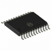
... Si4133 Package Outline: Si4133-BT Figure 19 illustrates the package details for the Si4133-BT. Table 16 lists the values for the dimensions shown in the illustration. D γ Figure 19. 24-Pin Thin Shrink Small Outline Package (TSSOP) Table 16. Package Diagram Dimensions Symbol *Note: To guarantee coplanarity ( θ Approximate device weight is 115.7 mg. ...
Page 33
... Package Outline: Si4133-BM Figure 20 illustrates the package details for the Si4133-BM. Table 17 lists the values for the dimensions shown in the illustration D TOP VIEW Figure 20. 28-Pin Micro Leadframe Package (MLP E1/2 E θ SECTION "C–C" SCALE: NONE e Table 17. Package Dimensions ...
Page 34
... Si4133 Document Change List Revision 1.3 to Revision 1.4 TSSOP outline updated. 34 Rev. 1.4 ...
Page 35
... Notes: Rev. 1.4 Si4133 35 ...
Page 36
... Si4133 Contact Information Silicon Laboratories Inc. 4635 Boston Lane Austin, Texas 78735 Tel:1+ (512) 416-8500 Fax:1+ (512) 416-9669 Toll Free: 1+ (877) 444-3032 Email: productinfo@silabs.com Internet: www.silabs.com The information in this document is believed to be accurate in all respects at the time of publication but is subject to change without notice. ...