DS1021S-25 Maxim Integrated Products, DS1021S-25 Datasheet
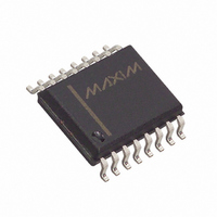
DELAY PROG 8-BIT 0.25NS 16-SOIC

DS1021S-25

Manufacturer Part Number
DS1021S-25
Description
DELAY PROG 8-BIT 0.25NS 16-SOIC
Manufacturer
Maxim Integrated Products
Datasheet

Specifications of DS1021S-25

Number Of Taps/steps
256
Function
Programmable
Delay To 1st Tap
10nS
Tap Increment
0.25nS
Available Total Delays
73.75ns
Voltage - Supply
4.75 V ~ 5.25 V
Operating Temperature
0°C ~ 70°C
Mounting Type
Surface Mount
Package / Case
16-SOIC (0.300", 7.5mm Width)
Lead Free Status / RoHS Status
Contains lead / RoHS non-compliant
Number Of Independent Delays
-
Other names
DS1021S25

Available stocks

Company
Part Number
Manufacturer
Quantity
Price
Part Number:
DS1021S-25
Manufacturer:
MAXIM
Quantity:
1 000
Part Number:
DS1021S-25
Manufacturer:
MAXIM/美信
Quantity:
20 000
Company:
Part Number:
DS1021S-25
Quantity:
900
Part Number:
DS1021S-25+T
Manufacturer:
DALLAS
Quantity:
20 000
Part Number:
DS1021S-25+T&R
Manufacturer:
MAXIM
Quantity:
3 942
Part Number:
DS1021S-25/T
Manufacturer:
SANYO
Quantity:
140
Part Number:
DS1021S-25/T&R
Manufacturer:
MAXIM
Quantity:
3 942
FEATURES
DESCRIPTION
The DS1021 Programmable 8-Bit Silicon Delay Line consists of an 8-bit, user-programmable CMOS
silicon integrated circuit. Delay values, programmed using either the 3-wire serial port or the 8-bit
parallel port, can be varied over 256 equal steps. The faster model (-25) offers a maximum delay of 73.75
ns with an incremental delay of 0.25 ns, while the slower model (-50) has a maximum delay of 137.5 ns
with an incremental delay of 0.5 ns. Both models have an inherent (step zero) delay of 10 ns. After the
user-determined delay, the input logic state is reproduced at the output without inversion. The DS1021 is
TTL- and CMOS-compatible, capable of driving 10 74LS-type loads, and features both rising and falling
edge accuracy.
The all-CMOS DS1021 integrated circuit has been designed as a reliable, economic alternative to hybrid
programmable delay lines. It is offered in a space-saving surface mount 16-pin SOIC.
www.dalsemi.com
All-silicon time delay
Models with 0.25 ns and 0.5 ns steps
Programmable using 3-wire serial port or 8-
bit parallel port
Leading and trailing edge accuracy
Economical
Auto-insertable, low profile, 16-pin SOIC
package
Low-power CMOS
TTL/CMOS-compatible
Vapor phase, IR and wave solderable
1 of 9
PIN ASSIGNMENT
PIN DESCRIPTION
IN
P0-P7
GND
OUT
V
S
E
C
Q
D
CC
DS1021S 16-Pin SOIC (300-mil)
See Mech. Drawings Section
Q/PO
GND
P3
P1
P2
P4
IN
E
Programmable 8-Bit
- Delay Input
- Parallel Program Pins
- Ground
- Delay Output
- +5 Volts
- Mode Select
- Enable
- Serial Port Clock
- Serial Data Output
- Serial Data Input
1
2
3
4
5
6
7
8
Silicon Delay Line
14
15
12
16
13
11
10
9
OUT
V
S
P6
P5
P7
C
D
CC
DS1021
111799

Related parts for DS1021S-25

DS1021S-25 Summary of contents

Page 1

... Silicon Delay Line PIN ASSIGNMENT Q/ GND 8 9 DS1021S 16-Pin SOIC (300-mil) See Mech. Drawings Section PIN DESCRIPTION IN - Delay Input P0-P7 - Parallel Program Pins GND - Ground OUT - Delay Output Volts Mode Select E - Enable C - Serial Port Clock Q - Serial Data Output D - Serial Data Input DS1021 ...

Page 2

PARALLEL MODE ( the PARALLEL programming mode, the output of the DS1021 will reproduce the logic state of the input after a delay determined by the state of the 8 program input pins P0 - P7. The ...

Page 3

FUNCTION BLOCK DIAGRAM Figure 1 SERIAL READOUT Figure 2 DS1021 ...

Page 4

CASCADING MULTIPLE DEVICES (DAISY CHAIN) Figure 3 PART NUMBER TABLE Table 1 PART NUMBER STEP ZERO DELAY TIME DS1020-25 10 ± 2 DS1020-50 10 ± 2 DELAY VS. PROGRAMMED VALUE Table 2 BINARY 0 PROGRAMMED 0 VALUE ...

Page 5

DALLAS SEMICONDUCTOR TEST CIRCUIT Figure 4 TEST SETUP DESCRIPTION Figure 4 illustrates the hardware configuration used for measuring the timing parameters of the DS1021. The input waveform is produced by a precision pulse generator under software control. Time delays are ...

Page 6

ABSOLUTE MAXIMUM RATINGS* Voltage on Any Pin Relative to Ground Operating Temperature Storage Temperature Soldering Temperature Short Circuit Output Current * This is a stress rating only and functional operation of the device at these or any other conditions above ...

Page 7

PARAMETER SYMBOL Parallel Input Change to Delay Invalid Enable to Delay Valid Enable to Delay Invalid V Valid to Device CC Functional V Rise Time CC Input Pulse Width Input to Output Delay Input Period CAPACITANCE PARAMETER SYMBOL Input ...

Page 8

TERMINOLOGY Period: The time elapsed between the leading edge of the first pulse and the leading edge of the following pulse. (Pulse Width): The elapsed time on the pulse between the 1.5V point on the leading edge and the t ...

Page 9

... TIMING DIAGRAM: POWER-UP Figure 9 NOTES: 1. All voltages are referenced to ground and 25°C. Delay accurate on both rising and falling edges within tolerances given in CC Table 1. 3. Measured with output open. 4. The “Q” output will only source 4 mA. This pin is only intended to drive other DS1021s ...

Related keywords