DS1033Z-10 Maxim Integrated Products, DS1033Z-10 Datasheet
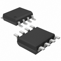
DELAY LINE 3TAP 10NS 8-SOIC

DS1033Z-10

Manufacturer Part Number
DS1033Z-10
Description
DELAY LINE 3TAP 10NS 8-SOIC
Manufacturer
Maxim Integrated Products
Datasheet

Specifications of DS1033Z-10

Function
Multiple
Delay To 1st Tap
10nS
Available Total Delays
10, 10, 10ns
Number Of Independent Delays
3
Voltage - Supply
2.7 V ~ 3.6 V
Operating Temperature
0°C ~ 70°C
Mounting Type
Surface Mount
Package / Case
8-SOIC (3.9mm Width)
Lead Free Status / RoHS Status
Contains lead / RoHS non-compliant
Number Of Taps/steps
-
Tap Increment
-
Other names
DS1033Z10

Available stocks

Company
Part Number
Manufacturer
Quantity
Price
Part Number:
DS1033Z-10
Manufacturer:
FUJI
Quantity:
1 000
Part Number:
DS1033Z-10
Manufacturer:
FUJI/富士电机
Quantity:
20 000
FEATURES
DESCRIPTION
The DS1033 series is a low-power +3.3 Volt version of the DS1035. It is characterized for operation
over the range of 2.7V to 3.6V.
The DS1033 series of delay lines have three independent logic buffered delays in a single package. It is
available in a standard 8-pin DIP, 150-mil 8-pin mini-SOIC.
The device features precise leading and trailing edge accuracies. It has the inherent reliability of an all-
silicon delay line solution. The DS1033’s nominal tolerance is 1.5 ns and an additional tolerance over
temperature and voltage of 1.0 ns for the faster delays. Detailed specifications are shown in Table 1.
Standard delay values are indicated in Table 1. Customers may contact Dallas Semiconductor at (972)
371-4348 for further information.
www.dalsemi.com
All-silicon timing circuit
Three independent buffered delays
Initial delay tolerance 1.5 ns
Stable and precise over temperature and
voltage
Leading and trailing edge precision preserves
the input symmetry
Standard 8-pin DIP, 8-pin SOIC
Vapor phasing, IR and wave solderable
Available in Tape and Reel
3-in-1 Low Voltage Silicon Delay Line
1 of 6
PIN ASSIGNMENT
PIN DESCRIPTION
IN1-IN3
OUT1-OUT3
NC
V
GND
(Sub)
CC
GND
DS1033Z 8-Pin SOIC (150-mil)
GND
IN1
IN2
IN3
See Mech. Drawings Section
IN1
IN2
IN3
DS1033M 8-Pin DIP
1
2
4
3
4
1
2
3
- Input Signals
- Output Signals
- No Connection
- Supply Voltage
- Ground
- Internal substrate
connection, do not make
any external connections
to these pins
8
7
5
6
5
8
7
6
V
OUT3
OUT1
OUT2
CC
V
OUT3
OUT1
OUT2
CC
DS1033
111799

Related parts for DS1033Z-10

DS1033Z-10 Summary of contents

Page 1

... Low Voltage Silicon Delay Line PIN ASSIGNMENT IN1 IN2 IN3 GND DS1033M 8-Pin DIP See Mech. Drawings Section IN1 IN2 IN3 GND DS1033Z 8-Pin SOIC (150-mil) See Mech. Drawings Section PIN DESCRIPTION IN1-IN3 OUT1-OUT3 GND (Sub DS1033 1 ...

Page 2

LOGIC DIAGRAM Figure 1 PART NUMBER DELAY TABLE (t DELAY PER OUTPUT (ns) PART NUMBER (note 1) DS1033-80 8/8/8 DS1033-10 10/10/10 DS1033-12 12/12/12 DS1033-15 15/15/15 DS1033-20 20/20/20 DS1033-25 25/25/25 DS1033-30 30/30/30 NOTES: 1. Nominal conditions are +25 C and V ...

Page 3

TEST SETUP DESCRIPTION Figure 2 illustrates the hardware configuration used for measuring the timing parameters of the DS1033. The input waveform is produced by a precision pulse generator under software control. Time delays are measured by a time interval counter ...

Page 4

ABSOLUTE MAXIMUM RATINGS* Voltage on Any Pin Relative to Ground Operating Temperature Storage Temperature Soldering Temperature Short Circuit Output Current * This is a stress rating only and functional operation of the device at these or any other conditions above ...

Page 5

TEST CONDITIONS Ambient Temperature: 3.3V =0.1V Supply Voltage ( Input Pulse: High: 3.0V =0.1V Low: 0.0V =0.1V Source Impedance: 50 =max. Rise and Fall Time: 3.0 ns max. - Measured between 0.6V and 2.4V. ...

Page 6

TERMINOLOGY Period: The time elapsed between the leading edge of the first pulse and the leading edge of the following pulse. t (Pulse Width): The elapsed time on the pulse between the 1.5 volt point on the leading edge and ...

Related keywords