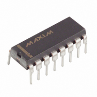
DS1020-100 Maxim Integrated Products, DS1020-100 Datasheet

DS1020-100
Specifications of DS1020-100
Available stocks
Related parts for DS1020-100
DS1020-100 Summary of contents
Page 1
... All models have an inherent (step-zero) delay of 10 ns. After the user-determined delay, the input logic state is reproduced at the output without inversion. The DS1020 is TTL- and CMOS-compatible, capable of driving 10 74LS-type loads, and features both rising and falling edge accuracy. ...
Page 2
... If the value read is restored before enable (E) is returned to logic 0, no settling time (t unchanged. Since the DS1020 is a CMOS design, unused input pins (P1 - P7) must be connected to well-defined logic levels; they must not be allowed to float. Serial output Q/P0 should be allowed to float if unused. and ground. For applications requiring ...
Page 3
FUNCTIONAL BLOCK DIAGRAM Figure 1 SERIAL READOUT Figure ...
Page 4
... DELAYS VS. PROGRAMMED VALUE Table 2 BINARY 0 PROGRAMMED 0 VALUE PART 0 NUMBER 0 DS1020-15 10.00 DS1020-25 10.00 DS1020-50 10.0 DS1020-100 10 DS1020-200 10 All delays in nanoseconds, referenced to input pin. DELAYS AND TOLERANCES (IN ns) MAX DELAY DELAY CHANGE TIME (NOM) PER STEP (NOM) 48.25 73.75 137.5 265 520 ...
Page 5
... The input waveform is produced by a precision pulse generator under software control. Time delays are measured by a time interval counter (20 ps resolution) connected to the output. The DS1020 serial and parallel ports are controlled by interfaces to a central computer. All measurements are fully automated with each instrument controlled by the computer over an IEEE 488 bus ...
Page 6
ABSOLUTE MAXIMUM RATINGS* Voltage on any Pin Relative to Ground Operating Temperature Storage Temperature Soldering Temperature Short Circuit Output Current * This is a stress rating only and functional operation of the device at these or any other conditions above ...
Page 7
PARAMETER SYMBOL Parallel Input Change to Delay Invalid Enable to Delay Valid Enable to Delay Invalid V Valid to Device CC Functional Input Pulse Width Input to Output Delay Input Period CAPACITANCE PARAMETER SYMBOL Input Capacitance TIMING DIAGRAM: SILICON ...
Page 8
TERMINOLOGY Period: The time elapsed between the leading edge of the first pulse and the leading edge of the following pulse. (Pulse Width): The elapsed time on the pulse between the 1.5V point on the leading edge and the t ...
Page 9
... TIMING DIAGRAM: SERIAL MODE ( Figure 8 NOTES: 1. All voltages are referenced to ground and 25°C. Delay accurate on both rising and falling edges within tolerances given in CC Table 1. 3. Measured with output open. 4. The “Q” output will only source 4 mA. This pin is only intended to drive other DS1020s ...


