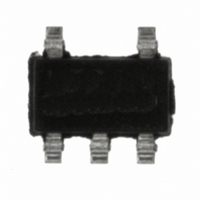
LTC6905CS5-133#TRMPBF Linear Technology, LTC6905CS5-133#TRMPBF Datasheet - Page 6

LTC6905CS5-133#TRMPBF
Manufacturer Part Number
LTC6905CS5-133#TRMPBF
Description
IC OSC PREC 133MHZ TSOT23-5
Manufacturer
Linear Technology
Type
Oscillator, Siliconr
Datasheet
1.LTC6905CS5-80TRMPBF.pdf
(8 pages)
Specifications of LTC6905CS5-133#TRMPBF
Frequency
133MHz
Voltage - Supply
2.7 V ~ 5.5 V
Current - Supply
10mA
Operating Temperature
-40°C ~ 85°C
Package / Case
TSOT-23-5, TSOT-5, TSOP-5
Lead Free Status / RoHS Status
Lead free / RoHS Compliant
Count
-
Other names
LTC6905CS5-133#TRMPBFTR
Available stocks
Company
Part Number
Manufacturer
Quantity
Price
LTC6905-XXX Series
APPLICATIO S I FOR ATIO
START-UP TIME
The start-up and settling time to within 1% of the final
frequency is typically 100µs.
MAXIMUM OUTPUT LOAD
The LTC6905 output (Pin 5) can drive a capacitive load
(C
greater than 5pF depends on the oscillator’s frequency
(f
or fall time due to R
C
total output rise time plus fall time is arbitrarily specified
to be equal to or less than 20% of the oscillator’s period (1/
f
should be equal to or less than [45454/(R
(R
Example: An LTC6905-100 is operating with a 3V power
supply and is set for a f
R
the Typical Performance Characteristics).
The maximum output C
than [45454/(27 • 50)] = 33.6pF.
The lowest resistive load Pin 5 can drive can be calculated
using the minimum high level output voltage in the Elec-
trical Characteristics. With a V
output current, the minimum high level output voltage is
5.2V and the lowest resistive load Pin 5 can drive is 1.30k
(5.2V/4mA). With a V
current, the minimum high level output voltage is 2.4V and
the lowest resistive load Pin 5 can drive is 600Ω (2.4V/4mA).
FREQUENCY ACCURACY AND POWER SUPPLY NOISE
The frequency accuracy of the LTC6905 may be affected
when its power supply generates noise with frequency
contents equal to f
highest frequency for an LTC6905-XXX which is with
DIV = V
part number (i.e., LTC6905-100, f
is the master oscillator control loop frequency. For ex-
ample, if the LTC6905-80 with a master oscillator fre-
quency of 80MHz is powered by a switching regulator,
6
OSC
LOAD
OSC
OUT
LOAD
OUT
), then the maximum output C
) and output resistance (R
with V
(from 10% to 90% of the rise or fall transition). If the
in ohms and f
) of 5pF or more. Performance driving a C
+
(÷1). This is also the frequency indicated in the
+
= 3V is 27Ω (using the R
U
OUT
OSC
MO
+
/64 or its multiples. f
and C
OSC
LOAD
in MHz).
equal to 2.7V and 4mA output
U
= 50MHz.
LOAD
should be equal to or less
OUT
+
equal to 5.5V and 4mA
MO
LOAD
is equal to 2.2 • R
). The output rise time
W
= 100MHz). f
OUT
in picofarads (pF)
vs V
OUT
U
MO
+
graph in
• f
MO
is the
OSC
OUT
LOAD
/64
)]
•
then the oscillator frequency may show an additional
error if the switching frequency is 1.4MHz (80MHz/64).
The magnitude of this effect is heavily dependent on
supply bypass and routing.
JITTER AND POWER SUPPLY NOISE
If the LTC6905 is powered by a supply that has frequency
content equal to the output frequency then the output jitter
may increase. In addition, power supply ripple in excess of
20mV at any frequency may increase jitter.
Higher divide ratios will result in lower percentage jitter.
For example, jitter percentage of the LTC6905-80 operat-
ing at 20MHz is lower than for the same part operating at
80MHz. Please consult the Jitter vs Frequency graph
showing jitter at various divider ratios.
LTC6905 SUGGESTED CRITICAL COMPONENT
LAYOUT
In order to provide the specified performance, it is re-
quired that the supply bypass capacitor be placed as close
as possible to the LTC6905. The following additional rules
should be followed for best performance:
1) The bypass capacitor must be placed as close as
2) If a ground plane is used, the connection of the LTC6905
possible to the LTC6905, and no vias should be placed
between the capacitor and the LTC6905. The bypass
capacitor must be on the same side of the circuit board
as the LTC6905.
to the ground plane should be as close as possible to the
LTC6905 GND pin and should be composed of multiple,
high current capacity vias.
Figure 2. LTC6905 Suggested Critical Component Layout
C
LTC6905
6905x F02
6905xfa


