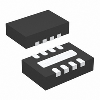
LTC6930HDCB-7.37#TRMPBF Linear Technology, LTC6930HDCB-7.37#TRMPBF Datasheet - Page 8

LTC6930HDCB-7.37#TRMPBF
Manufacturer Part Number
LTC6930HDCB-7.37#TRMPBF
Description
IC OSCILLATOR PREC LP 8-DFN
Manufacturer
Linear Technology
Type
Oscillator, Siliconr
Datasheet
1.LTC6930CDCB-7.37TRMPBF.pdf
(14 pages)
Specifications of LTC6930HDCB-7.37#TRMPBF
Frequency
7.3728MHz
Voltage - Supply
1.7 V ~ 5.5 V
Current - Supply
853µA
Operating Temperature
-40°C ~ 125°C
Package / Case
8-DFN
Lead Free Status / RoHS Status
Lead free / RoHS Compliant
Count
-
Available stocks
Company
Part Number
Manufacturer
Quantity
Price
PIN FUNCTIONS
LTC6930-X.XX
V
should be bypassed directly to the neighboring GND pin
with a 0.1µF ceramic capacitor, and must be externally
connected to the other V
GND (Pins 2, 6): Ground Pins. Each should be connected
to a low inductance ground plane and must be connected
to the other GND pin and on the DFN package, Pin 9.
DIVA, DIVB, DIVC (Pins 3, 4, 5): Output Prescaler. Se-
lects divide ratio of master oscillator frequency used to
generate the output. See frequency setting Table 1 for
function. These are standard CMOS logic inputs with a
typical threshold of 1.25V
APPLICATIONS INFORMATION
Theory of Operation
The LTC6930 is an entirely self contained all silicon oscil-
lator which consists of a master oscillator, a control loop
and an output frequency divider. The master oscillator
operates between 4.2MHz and 8.2MHz and is factory
programmed. The master oscillator frequency is accurately
maintained over temperature and environmental extremes
by a proprietary switched capacitor feedback loop.
Each LTC6930 oscillator has an output frequency divider
which is controlled via the DIVA, DIVB and DIVC inputs.
The divider divides the master frequency by 2
is an integer from 0 to 7 (divider ranges from 1 to 128).
See Table 1 for the full range of frequencies covered by
the LTC6930 family.
The presence of two sets of supply pins and careful internal
layout reduce interference between the oscillator output
and the control loop. This allows the LTC6930 to provide
a clean output frequency with very little deterministic jitter,
even in cases of heavy output loading and noisy operating
environments.
The supply voltage of the LTC6930 is internally regulated
to maintain a very low frequency drift over supply.
8
+
(Pins 1, 8): Positive Supply Pins. Each supply pin
+
pin (see recommended layout).
N
, where N
OUT (Pin 7): Oscillator Output. Drives up to 50pF capaci-
tive or 1k resistive load (Refer to Supply Current vs Load
Capacitance in Typical Performance Characteristics sec-
tion). Typical series resistance is less than 80Ω at 1.7V
and less than 40Ω at 3V supply. The output trace should
be isolated as much as possible from Pin 1 and Pin 2.
The OUT pin is held low during start-up, and remains free
from glitches and runt pulses during DIV pin switching.
Exposed Pad (Pin 9, DFN Only): The Exposed Pad must
be soldered to a PCB plane connected to GND.
Output Driver and Loading
The output of the LTC6930 is a low series resistance 40Ω
CMOS driver with controlled rise/fall times to limit RF
interference and power supply spikes generated by the
output while preserving the ability to drive low impedance
loads. Especially at high frequencies, the capacitive loading
of the output of the LTC6930 may cause the majority of
the power supply dissipation of the part.
The LTC6930 supply current is specified at an output load
of 5pF , which is equivalent to two standard HC logic inputs.
The portion of the power supply current needed to drive
a capacitive load may be calculated as:
where C
voltage swing, in this case up to 5.5V, and f
quency of the oscillator output. Driving a 5.5V swing into a
5pF load at 8MHz takes an average of 220µA. To calculate
the portion of the supply current needed for a 50pF load,
simply substitute 50pF for C
The majority of this power is expended during the rise and
fall time of the output signal, not while it is in a steady
I
50pF • 5.5V • 8MHz = 2.2mA
SUPPLY
LOAD
= C
is the 5pF load capacitance, V
LOAD
• V
SWING
LOAD
• f
OSC
in the same equation:
OSC
SWING
is the fre-
is the
6930fd


