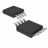
LTC6903CMS8 Linear Technology, LTC6903CMS8 Datasheet - Page 8

LTC6903CMS8
Manufacturer Part Number
LTC6903CMS8
Description
IC OSC PROGRAM SPI SERIAL 8-MSOP
Manufacturer
Linear Technology
Type
Oscillator, Siliconr
Specifications of LTC6903CMS8
Frequency
68MHz
Voltage - Supply
2.7 V ~ 5.5 V
Current - Supply
7mA
Operating Temperature
-40°C ~ 85°C
Package / Case
8-MSOP, Micro8™, 8-uMAX, 8-uSOP,
Lead Free Status / RoHS Status
Contains lead / RoHS non-compliant
Count
-
Lead Free Status / Rohs Status
Not Compliant
Available stocks
Company
Part Number
Manufacturer
Quantity
Price
Part Number:
LTC6903CMS8
Manufacturer:
LINEAR/凌特
Quantity:
20 000
Company:
Part Number:
LTC6903CMS8#TRPBF
Manufacturer:
FOXCONN
Quantity:
1 000
LTC6903/LTC6904
applicaTions inFormaTion
Additionally, the LTC6903/LTC6904 is guaranteed to be
monotonic when switching between octaves with the
OCT setting bits. For example, the frequency output with
a DAC setting of “1111111111” and an OCT setting of
“1100” will always be lower than the frequency output
with a DAC setting of “0000000000” and an OCT setting
of “1101”. Linearity at these transition points is typically
around 3 LSBs.
Output Loading and Accuracy
Improper loading of the outputs of the LTC6903/LTC6904,
especially with poor power supply bypassing, will result in
accuracy problems. At low frequencies, capacitive loading
of the output is not a concern. At frequencies above 1MHz,
attention should be paid to minimize the capacitive load
on the CLK and CLK pins.
The LTC6903/LTC6904 is designed to drive up to 5pF
on each output with no degradation in accuracy. 5pF is
equivalent to one to two HC series logic inputs. A standard
10x oscilloscope probe usually presents between 10pF
and 15pF of capacitive load.
It is strongly suggested that a high speed buffer is used
when driving more than one or two logic inputs, when
driving a line more than 5 centimeters in length, or a
capacitive load greater than 5pF .
SEN
SCK
SDI
D15
D14
D13
D12
D11
D10
Timing Diagram (LTC6903)
D9
D8
Output Control
The CLK and CLK outputs of the LTC6903/LTC6904 are
individually controllable through the serial port as de-
scribed in Table 2 below. The low power mode may also
be accessed through these control bits. It is preferred
that unused outputs be disabled in order to reduce power
dissipation and improve accuracy.
Disabling an unused output will improve accuracy of
operation at frequencies above 1MHz. An unused output
running with no load typically degrades frequency ac-
curacy up to 0.2% at 68MHz. An unused output running
into a 5pF load typically degrades frequency accuracy up
to 0.5% at 68MHz.
Table 2. Output Configuration
*Powered-Down: When in this mode, the chip is in a low power state
and will require approximately 100µs to recover. This is not the same
effect as the OE pin, which is fast, but uses more power supply current.
Serial Port Bitmap (LTC6903/LTC6904)
(All serial port register bits default LOW at power up)
Table 3
OCT3
DAC5
D15
D7
D7
CNF1
0
0
1
1
D6
OCT2
DAC4
D14
D6
D5
OCT1
DAC3
D13
D5
CNF0
D4
0
1
0
1
DAC2
OCT0
D12
D4
D3
DAC9
DAC1
D11
D3
D2
CLK
OFF
ON
ON
Powered-Down*
DAC8
DAC0
D10
D2
D1
DAC7
CNF1
D0
D9
D1
CLK + 180°
CLK
OFF
ON
DAC6
CNF0
6903 TD01
69034fc
D8
D0


