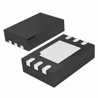
LTC6908IDCB-1#TRPBF Linear Technology, LTC6908IDCB-1#TRPBF Datasheet - Page 6

LTC6908IDCB-1#TRPBF
Manufacturer Part Number
LTC6908IDCB-1#TRPBF
Description
IC OSC PREC LP RES SET 6-DFN
Manufacturer
Linear Technology
Type
Oscillator, Siliconr
Datasheet
1.LTC6908CS6-2TRPBF.pdf
(16 pages)
Specifications of LTC6908IDCB-1#TRPBF
Frequency
10MHz
Voltage - Supply
2.7 V ~ 5.5 V
Current - Supply
1.25mA
Operating Temperature
-40°C ~ 85°C
Package / Case
6-DFN
Lead Free Status / RoHS Status
Lead free / RoHS Compliant
Count
-
Available stocks
Company
Part Number
Manufacturer
Quantity
Price
BLOCK DIAGRA
LTC6908-1/LTC6908-2
PI FU CTIO S
SET (Pin 1/Pin 3): Frequency-Setting Resistor Input. The
value of the resistor connected between this pin and V
determines the oscillator frequency. The voltage on this pin
is held by the LTC6908 to approximately 1.1V below the
V
fi lm resistor with a value between 20k and 400k and limit
the capacitance on this pin to less than 10pF.
V
supply must be kept free from noise and ripple. It should
be bypassed directly to a ground plane with a 0.1µF
capacitor.
GND (Pin 3/Pin 2): Ground. Should be tied to a ground
plane for best performance.
OUT1 (Pin 4/Pin 6), OUT2 (Pin 5/Pin 5): Oscillator Out-
puts. These pins can drive 5k and/or 10pF loads. Larger
loads may cause inaccuracies due to supply bounce at
high frequencies.
6
+
+
U
(Pin 2/Pin 1): Voltage Supply (2.7V ≤ V
voltage. For best performance, use a precision metal
R
SET
MOD
SET
V
+
U
1
3
4
V
–
–
+
+
BIAS
GND
V
+
U
2µA
2µA
–
+
W
GAIN = 1
(DCB Package/S6 Package)
I
SET
INPUT DECODER
CLOCK INPUT
(S6 Package Pin Numbers)
=
3-STATE
DETECT
V
MDAC
+
V
– V(SET)
R
+
SET
– V(SET) ≈ 1.13V
I
REF
+
CODE GENERATOR
PSEUDO RANDOM
WHEN A CLOCK SIGNAL IS PRESENT AT THE
MOD INPUT, DISABLE THE MODULATION.
≤ 5.5V). This
f
MASTER
1-POLE
LPF
= 20MHz • 10k •
DIVIDER SELECT
CLK
+
V
I
MASTER
MOD (Pin 6/Pin 4): Modulation-Setting Input. This three-
state input selects among four modulation rate settings.
The MOD pin should be tied to ground for the f
modulation rate. Floating the MOD pin selects the f
modulation rate. The MOD pin should be tied to V
f
MOD pin turns the modulation off. To detect a fl oating
MOD pin, the LTC6908 attempts to pull the pin toward
midsupply. This is realized with two internal current
sources, one tied to V
to ground and MOD. Therefore, driving the MOD pin high
requires sourcing approximately 2µA. Likewise, driving the
MOD pin low requires sinking 2µA. When the MOD pin is
fl oated, it must be bypassed by a 1nF capacitor to ground.
Any AC signal coupling to the MOD pin could potentially
be detected and stop the frequency modulation.
Exposed Pad (Pin 7/NA): Ground. The Exposed Pad must
be soldered to PCB.
OSCILLATOR
V
OUT
+
MASTER
I
MASTER
– V(SET)
/64 modulation rate. Tying one of the outputs to the
= 20MHz • 10k/R
OUT
DIVIDE BY
16/32/64
COMPLEMENTARY
SET
MUTE OUTPUT
QUADRATURE
UNTIL STABLE
OUTPUTS
POR
OR
+
and MOD and the other one tied
90/180
0
f
OUT
= f
MASTER
690812 BD
/2
6
5
2
OUT1
OUT2
GND
+
OUT
OUT
for the
690812fa
/16
/32


