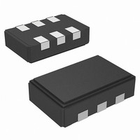
CY2XF34FLXCT Cypress Semiconductor Corp, CY2XF34FLXCT Datasheet

CY2XF34FLXCT
Specifications of CY2XF34FLXCT
Related parts for CY2XF34FLXCT
CY2XF34FLXCT Summary of contents
Page 1
... LVPECL Output 6 VDD Power 3 VSS Power Cypress Semiconductor Corporation Document Number: 001-53149 Rev. *D High Performance LVPECL Oscillator with Frequency Margining - Pin Control Functional Description The CY2XF34 is a high performance and high frequency Crystal Oscillator (XO). It uses a Cypress proprietary low noise PLL to synthesize the frequency from an integrated crystal ...
Page 2
Functional Description The FS0 and FS1 pins select between four different output frequencies, as shown in Table 1. Frequency margining is a common application for this feature. One frequency is used for the standard operating mode of the device, while ...
Page 3
Absolute Maximum Conditions Parameter Description V Supply Voltage DD [1] V Input Voltage Temperature, Storage S T Temperature, Junction J ESD ESD Protection (Human Body Model) HBM [2] Thermal Resistance, Junction to Ambient JA Operating Conditions ...
Page 4
DC Electrical Characteristics Parameter Description [4] C Input Capacitance, FS0 pin IN0 [4] C Input Capacitance, FS1 pin IN1 AC Electrical Characteristics The AC Electrical Characteristics for part CY2XF34 are as follows Parameter Description [5] F Output Frequency OUT FSC ...
Page 5
Figure 3. 2.5 V Supply and Termination to V 0.9 0.8 0.7 0.6 0.5 0.4 0 100 200 300 400 Frequency (MHz) Figure 4. 3.3 V Supply and Termination to V 0.9 0.8 0.7 0.6 0.5 0.4 0 100 200 ...
Page 6
Switching Waveforms CLK CLK# CLK CLK# Termination Circuits CLK CLK# Document Number: 001-53149 Rev. *D Figure 5. Output DC Parameters V OD Figure 6. Duty Cycle Timing PERIOD Figure 7. Output Rise and Fall ...
Page 7
... Ordering Information Part Number Configuration Pb-Free CY2XF34FLXCT Field Programmable CY2XF34FLXIT Field Programmable Possible Cofigurations Some product offerings are factory programmed customer specific devices with customized part numbers.The Possible Configurations table shows the available device types, but not complete part numbers. Contact your local Cypress FAE of Sales Representative for more information ...
Page 8
Package Drawings and Dimensions Figure 9. 6-pin 3.2 × 5.0 mm Ceramic LCC LZ06A Document Number: 001-53149 Rev. *D CY2XF34 001-10044 *A Page [+] Feedback ...
Page 9
Acronyms Acronym Description CMOS complementary metal oxide semiconductor ESD electrostatic discharge FAE Field Application Engineer I/O input/output OTP One Time Programmable PCB printed circuit board PLL phase-locked loop SMD Surface Mounted Devices Document Number: 001-53149 Rev. *D Document Conventions Units ...
Page 10
... Cypress against all charges. Any Source Code (software and/or firmware) is owned by Cypress Semiconductor Corporation (Cypress) and is protected by and subject to worldwide patent protection (United States and foreign), United States copyright laws and international treaty provisions. Cypress hereby grants to licensee a personal, non-exclusive, non-transferable license to copy, use, modify, create derivative works of, and compile the Cypress Source Code and derivative works for the sole purpose of creating custom software and or firmware in support of licensee product to be used only in conjunction with a Cypress integrated circuit as specified in the applicable agreement ...


