DS4625P+100/150 Maxim Integrated Products, DS4625P+100/150 Datasheet

IC OSC CLOCK 100-150MHZ 10-LCCC

DS4625P+100/150

Manufacturer Part Number
DS4625P+100/150
Description
IC OSC CLOCK 100-150MHZ 10-LCCC
Manufacturer
Maxim Integrated Products
Type
Clock Oscillatorr
Datasheet

Specifications of DS4625P+100/150

Frequency
150MHz
Voltage - Supply
2.97 V ~ 3.63 V
Current - Supply
120mA
Operating Temperature
-40°C ~ 85°C
Package / Case
10-LCCC
Number Of Internal Timers
1
Supply Voltage (max)
3.63 V
Supply Voltage (min)
2.97 V
Maximum Operating Temperature
+ 70 C
Minimum Operating Temperature
- 40 C
Mounting Style
SMD/SMT
Propagation Delay (max)
100 ns
Lead Free Status / RoHS Status
Lead free / RoHS Compliant
Count
-
Lead Free Status / Rohs Status
Lead free / RoHS Compliant
The DS4625 is a dual-output, low-jitter clock oscillator
capable of producing frequency output pair combina-
tions ranging from 100MHz to 625MHz. The device
combines an AT-cut crystal, an oscillator, and a low-
noise phase-locked loop (PLL) in a 5.0mm x 3.2mm
surface-mount LCCC package. Standard frequency
options are listed in the Ordering Information/Selector
Guide table. For custom frequency options, contact the
factory at: Custom.Oscillators@maxim-ic.com.
The DS4625 provides dual, low-voltage, positive emit-
ter-coupled logic (LVPECL) clock output drivers. The
output drivers can be enabled and disabled through
the OE pin, which is an active-high CMOS input that
has an internal pullup resistor. When high, both output
pairs are enabled.
The device operates from a single +3.3V ±10% supply.
The operating temperature range is -40°C to +85°C.
+ Denotes a lead(Pb)-free/RoHS-compliant package. The lead finish is JESD97 category e4 (Au over Ni) and is compatible with both
lead-based and lead-free soldering processes.
* Standard frequency options. Contact the factory at
19-4558; Rev 1; 3/10
Pin Configuration and Typical Application Circuit appear at end of data sheet.
InfiniBand is a trademark and service mark of the InfiniBand Trade Association.
PCIe is a registered trademark of PCI-SIG Corp.
For pricing, delivery, and ordering information, please contact Maxim Direct at 1-888-629-4642,
or visit Maxim’s website at www.maxim-ic.com.
DS4625P+100/100
DS4625P+100/150
DS4625P+125/125
DS4625P+125/156
DS4625P+150/150
DS4625P+150/200
XGMII Clock Oscillator
InfiniBand
SAS/SATA
PCIe
1GbE/10GbE
PART
®
3.3V Dual-Output LVPECL Clock Oscillator
TM/SM
________________________________________________________________ Maxim Integrated Products
-40°C to +85°C
-40°C to +85°C
-40°C to +85°C
-40°C to +85°C
-40°C to +85°C
-40°C to +85°C
TEMP RANGE
General Description
Applications
FREQUENCY (OP1:ON1)
Custom.Oscillators@maxim-ic.com
(MHz) (f
100.000
100.000
125.000
125.000
150.000
150.000
C
)*
Ordering Information/Selector Guide
♦ Standard Clock Output Frequencies: 100MHz,
♦ Phase Jitter < 0.7ps RMS (typical) from 12kHz to
♦ LVPECL Output
♦ +3.3V ±10% Operating Voltage
♦ -40°C to +85°C Temperature Range
♦ Excellent Power-Supply Noise Rejection
♦ 5.0mm x 3.2mm Ceramic LCCC Package
♦ Output Enable/Disable
125MHz, 150MHz, 156.25MHz, and 200MHz
20MHz
FREQUENCY (OP2:ON2)
(MHz) (f
100.000
150.000
125.000
156.250
150.000
200.000
for custom frequencies.
C
)*
PIN-PACKAGE
10 LCCC
10 LCCC
10 LCCC
10 LCCC
10 LCCC
10 LCCC
Features
MARK
TOP
6CC
6AA
6AC
6BB
6BD
6CE
1

Related parts for DS4625P+100/150

DS4625P+100/150 Summary of contents

Page 1

... TM/SM InfiniBand SAS/SATA ® PCIe 1GbE/10GbE PART TEMP RANGE DS4625P+100/100 -40°C to +85°C DS4625P+100/150 -40°C to +85°C DS4625P+125/125 -40°C to +85°C DS4625P+125/156 -40°C to +85°C DS4625P+150/150 -40°C to +85°C DS4625P+150/200 -40°C to +85°C + Denotes a lead(Pb)-free/RoHS-compliant package. The lead finish is JESD97 category e4 (Au over Ni) and is compatible with both lead-based and lead-free soldering processes ...

Page 2

Dual-Output LVPECL Clock Oscillator ABSOLUTE MAXIMUM RATINGS (All voltages referenced to ground unless otherwise noted.) Voltage Range on Any Pin Relative to Ground......-0.3V to +4.0V Operating Temperature Range ...........................-40°C to +85°C Junction Temperature ......................................................+150°C Note 1: Package thermal resistances ...

Page 3

Dual-Output LVPECL Clock Oscillator ELECTRICAL CHARACTERISTICS (continued +2.97V to +3.63V -40°C to +85°C, typical values are PARAMETER SYMBOL Output High Voltage Output Low Voltage Differential Output Voltage Output Rise Time Output ...

Page 4

Dual-Output LVPECL Clock Oscillator (T = +25°C, unless otherwise noted DEVIATION vs. TEMPERATURE -10 -20 -30 -40 -50 -40 - TEMPERATURE (°C) PIN NAME 1 OE ...

Page 5

Dual-Output LVPECL Clock Oscillator X1 X0 PLL X2 DS4625 Figure 1. Block Diagram 0 OP_ PECL_BIAS ON_ PECL_BIAS Figure 2. LVPECL Output Timing Diagram When OE is Enabled and Disabled _______________________________________________________________________________________ V CC LC-VCO PFD ...

Page 6

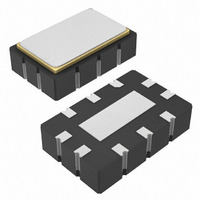
Dual-Output LVPECL Clock Oscillator Pin Configuration TOP VIEW N.C. N. GND 2 DS4625 GND 3 * OP2 ON2 (5.00mm × 3.20mm × 1.49mm) *EXPOSED PAD 0.1μF 6 _______________________________________________________________________________________ The DS4625 is a ...

Page 7

... Maxim cannot assume responsibility for use of any circuitry other than circuitry entirely embodied in a Maxim product. No circuit patent licenses are implied. Maxim reserves the right to change the circuitry and specifications without notice at any time. Maxim Integrated Products, 120 San Gabriel Drive, Sunnyvale, CA 94086 408-737-7600 _____________________ 7 © 2010 Maxim Integrated Products ...

Related keywords