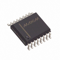
DS4026S+YCN Maxim Integrated Products, DS4026S+YCN Datasheet - Page 10

DS4026S+YCN
Manufacturer Part Number
DS4026S+YCN
Description
IC TXCO 19.6608MHZ 16-SOIC
Manufacturer
Maxim Integrated Products
Type
Temperature, Compensated Crystal Oscillator (TCXO)r
Datasheet
1.DS4026SYCN.pdf
(14 pages)
Specifications of DS4026S+YCN
Frequency
19.6608MHz
Voltage - Supply
3.135 V ~ 3.465 V
Current - Supply
1.5mA
Operating Temperature
-40°C ~ 85°C
Package / Case
16-SOIC (0.300", 7.5mm Width)
Lead Free Status / RoHS Status
Lead free / RoHS Compliant
Count
-
In the temperature register (see the Temperature
Register (02h–03h) table), temperature is represented
as a 12-bit code and is accessible at location 02h and
03h. The upper 8 bits are at location 02h and the lower
4 bits are in the upper nibble of the byte at location
03h. Upon power reset, the registers are set to a +25°C
default temperature and the controller starts a tempera-
ture conversion. The temperature register stores new
temperature readings.
The current temperature is loaded into the (user) tem-
perature registers when a valid I
write is received and when a word address is received.
Consequently, if the two temperature registers are read
in individual I
perature conversion to occur between reads, and the
results can be inaccurate. To prevent this from occur-
ring, the registers should be read using a single, multi-
byte read operation (Figure 5). I
the internal temperature registers.
10MHz to 51.84MHz TCXO
Table 1. Register Map
Figure 3. I
10
ADDRESS
SDA
SCL
CONDITION
00
01
02
03
______________________________________________________________________________________
START
2
C Data Transfer Overview
DCOMP
BIT 7
2
SIGN
C transactions, it is possible for a tem-
MSB
1
BIT 6
SIGN
2
SLAVE ADDRESS
2
2
C reads do not affect
C slave address and
BIT 5
6
Read Mode
7
BIT 4
DIRECTION
R/W
BIT
8
SIGNAL FROM RECEIVER
ACKNOWLEDGEMENT
FTUNEH
FTUNEL
TREGH
TREGL
BIT 3
ACK
9
The DS4026 supports a bidirectional I
transmission protocol. A device that sends data onto
the bus is defined as a transmitter and a device receiv-
ing data is defined as a receiver. The device that con-
trols the message is called a master. The devices that
are controlled by the master are slaves. The bus must
be controlled by a master device that generates the
serial clock (SCL), controls the bus access, and gener-
ates the START and STOP conditions. The DS4026
operates as a slave on the I
bus are made through the open-drain I/O lines SDA
and SCL. Within the bus specifications, a standard
mode (100kHz maximum clock rate) and a fast mode
(400kHz maximum clock rate) are defined. The DS4026
works in both modes.
The following bus protocol has been defined (Figure 3):
• Data transfer can be initiated only when the bus is
not busy.
BIT 2
1
BIT 1
2
REPEATED IF MORE BYTES
ARE TRANSFERED
3–7
I
SIGNAL FROM RECEIVER
BIT 0
ACKNOWLEDGEMENT
2
C Serial Data Bus
8
2
C bus. Connections to the
Frequency Tuning High
Frequency Tuning Low
Temperature MSB
Temperature LSB
ACK
9
2
FUNCTION
C bus and data
OR REPEATED
CONDITION
CONDITION
START
STOP


