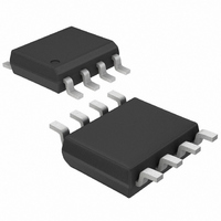
DS1388Z-5+ Maxim Integrated Products, DS1388Z-5+ Datasheet - Page 16

DS1388Z-5+
Manufacturer Part Number
DS1388Z-5+
Description
IC RTC I2C W/CHARGER 8-SOIC
Manufacturer
Maxim Integrated Products
Type
Clock/Calendar/Supervisor/EEPROMr
Datasheet
1.DS1388Z-33.pdf
(19 pages)
Specifications of DS1388Z-5+
Memory Size
4K (512 x 8)
Time Format
HH:MM:SS:hh (12/24 hr)
Date Format
YY-MM-DD-dd
Interface
I²C, 2-Wire Serial
Voltage - Supply
4.5 V ~ 5.5 V
Operating Temperature
-40°C ~ 85°C
Mounting Type
Surface Mount
Package / Case
8-SOIC (3.9mm Width)
Lead Free Status / RoHS Status
Lead free / RoHS Compliant
The slave address byte is the first byte received follow-
ing the START condition from the master device. The
slave address byte consists of a 4-bit control code. For
the DS1388, this is set as 1101 binary for read and
write operations. The next three bits of the slave
address byte are the block select bits (B2, B1, B0). B2
is always logic 0 for the DS1388. These bits are used
by the master device to select which of the three blocks
in the memory map are to be accessed. These bits are
the three most significant bits of the word address. The
last bit of the slave address byte defines the operation
to be performed. When set to 1, a read operation is
selected; when set to 0, a write operation is selected.
Following the START condition from the master, the
device code (4 bits); the block address (3 bits); and the
R/W bit, which is logic-low, is placed onto the bus by
the master transmitter. This indicates to the DS1388
that a byte with a word address follows after the
DS1388 has generated an acknowledge bit during the
ninth clock cycle. The next byte transmitted by the
master is the word address and will set the internal
address pointer of the DS1388, with the DS1388
acknowledging the transfer on the ninth clock cycle.
The master device can then transmit zero or more
bytes of data, with the DS1388 acknowledging the
transfer on the ninth clock cycle. The master generates
a STOP condition to terminate the data write.
The write-slave address byte and word address are
transmitted to the DS1388 as described in the Slave
I
and 512 Bytes EEPROM
16
2
C RTC/Supervisor with Trickle Charger
BIT 7
Read Upper Block of EEPROM
Read Lower Block of EEPROM
Write Lower Block of EEPROM
Write Upper Block of EEPROM
____________________________________________________________________
1
Slave Receiver Mode (Write Mode)
OPERATION
Read Clock
Write Clock
BIT 6
1
Device Addressing
Write Operation
BIT 5
0
Byte Write
CONTROL CODE
BIT 4
1
1101
1101
1101
1101
1101
1101
Receiver Mode section. The master transmits one data
byte, with the DS1388 acknowledging the transfer on
the ninth clock cycle. The master then generates a
STOP condition to terminate the data write. This initiates
the internal write cycle, and, if the write was to the
EEPROM, the DS1388 does not generate acknowledge
signals during the internal EEPROM write cycle.
The write-slave address byte, word address, and the
first data byte are transmitted to the DS1388 in the
same way as in a byte write. But instead of generating
a STOP condition, the master transmits up to 8 data
bytes to the DS1388, which are temporarily stored in
the on-chip page buffer and are written into the memo-
ry after the master has transmitted a STOP condition.
Data bytes within the page that are not written remain
unchanged. The internal address pointer automatically
increments after each byte is written.
If the master should transmit more than 8 data bytes prior
to generating the STOP condition, the address pointer
rolls over and the previously received data is overwritten.
As with the byte write operation, once the STOP condi-
tion is received an internal write cycle begins.
Writing multiple bytes to the RTC works much the same
way as the EEPROM page write, except that the entire
contents of block 0h can be written at once. The 8-byte
page size limitation does not apply to the block 0. If the
master should transmit more bytes than exists in block
0 prior to generating the STOP condition, the internal
address pointer rolls over and the previously received
data is overwritten. As with the byte write operation,
once the STOP condition is received an internal write
cycle begins.
BIT 3
B2
BLOCK SELECT
BIT 2
B1
000
000
001
001
010
010
Slave Address Byte
EEPROM Page Write
RTC Multibyte Write
BIT 1
B0
R/W
BIT 0
R/W
1
0
1
0
1
0


