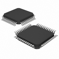
DS1558W+ Maxim Integrated Products, DS1558W+ Datasheet - Page 8

DS1558W+
Manufacturer Part Number
DS1558W+
Description
IC RTC W/NV RAM 3.3V 48-LQFP
Manufacturer
Maxim Integrated Products
Type
Watchdog Timer/NVSRAMr
Datasheet
1.DS1558W.pdf
(18 pages)
Specifications of DS1558W+
Time Format
HH:MM:SS (24 hr)
Date Format
YY-MM-DD-dd
Interface
Parallel
Voltage - Supply
3 V ~ 3.6 V
Operating Temperature
-40°C ~ 85°C
Mounting Type
Surface Mount
Package / Case
48-LQFP
Lead Free Status / RoHS Status
Lead free / RoHS Compliant
Memory Size
-
READING THE CLOCK
When reading the RTC data, it is recomme ed to halt updates to the external set
RTC registers. This puts the external registers into a static state, allowing data to be re
values changing during the read process. Normal updates to the internal registers con
state. External updates are halted when a 1 is written into the read bit, B6 of t
(7FFF8h). As long as a 1 remains in the control register read bit, updating is halted. Af
the registers reflect the RTC count (day, date, and time) that was current at the moment
is issued. Normal updates to the external se f registers
a 0 for a minimum of 500
registers are updated.
SETTING THE CLOCK
The MSB bit, B7, of the control register is the write bit. Setting the write bit to a 1, lik
updates to the 7FFF8h–7FFFFh registers. After setting the write bit to a 1, RTC registers can be loaded
with the desired RTC count (day, date, and time) in 24-hour BCD format. Setting the w
transfers the values written to the internal RTC registers and allows normal operation to
CLOCK ACCURACY
The accurac
between the capacitive load of the oscillator circuit and the capacitive
trimmed. Additional error is added by the crystal-frequency drift caused
circuit noise coupled int
Note 58 “Crystal Considerations with Dallas Real-Time Clocks” for detailed informatio
FREQUENCY TEST MODE
The DS1558 frequency test mode uses the open-drain
watchdog-enable bit (WDS) is a 1, o
output and the frequency test mode can be used as a measure of the actual frequency
RTC oscillator. The
operation. The FT bit is cleared to a 0 on power-up.
USING THE CLOCK ALARM
The alarm settings and control for the DS1558 reside within registers 7FFF2h–7FFF5h
contains two alarm-enable bits: alarm enable (AE) and alarm in backup enable (ABE).
bits must be set as described below for the
The alarm can be programmed to activate on a specific day of the month or repeat every day, hour,
minute, or second. It can also be programmed to go off while the DS1558 is in the battery-backed state of
operation to serve as a system wake-up. Alarm mask bits AM1–AM4 control the alarm mode. Table 3
shows the possible settings. Configurat
notify the user of an incorrect alarm setting.
IRQ
/FT output toggles at 512Hz when the FT bit is a 1, the alarm-flag enable bit (AE) is a 0, and the
y of the clock is dependent upon the accuracy of the crystal and the accuracy of the match
IRQ
o the oscillator circuit can result in the clock running fast. Refer to Application
/FT pin is an open-drain output that requires a pullup resistor for proper
s. The read bit m
r the watchdog register is reset (register 7FFF7h = 00h). The
ions not listed in the table default to the once-per-second mode to
IRQ
t
o
nd
u
/FT output to be activated for a matched alarm condition.
st be a 0 for a m
8 of 18
re
IRQ
s
ume within 1 second after the read bit is set to
/FT output. With the oscillator running, the
inimum of 500 s to ensure the extern
load for which the crystal was
by temperature shifts. External
he control register
of double-buffered
e the read bit, halts
ad without register
t
tinue while in this
n.
. Register 7FFF6h
er a
The AE and ABE
the h
rite bit to a 0 then
resume.
of the 32.768kHz
halt is issued,
alt com
IRQ
mand
/FT
al


