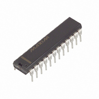
DS17287-5+ Maxim Integrated Products, DS17287-5+ Datasheet - Page 22

DS17287-5+
Manufacturer Part Number
DS17287-5+
Description
IC RTC 5V 2K NV RAM 24-EDIP
Manufacturer
Maxim Integrated Products
Type
Clock/Calendar/NVSRAMr
Datasheet
1.DS17287-5.pdf
(31 pages)
Specifications of DS17287-5+
Memory Size
16K (2K x 8)
Time Format
HH:MM:SS (12/24 hr)
Date Format
YY-MM-DD-dd
Interface
Parallel
Voltage - Supply
4.5 V ~ 5.5 V
Operating Temperature
0°C ~ 70°C
Mounting Type
Through Hole
Package / Case
24-DIP (600 mil) Module
Function
Clock/Calendar/Alarm
Rtc Memory Size
2048 Byte
Supply Voltage (max)
5.5 V
Supply Voltage (min)
4.5 V
Maximum Operating Temperature
+ 70 C
Minimum Operating Temperature
0 C
Mounting Style
Through Hole
Rtc Bus Interface
Multiplexed
Supply Current
25 mA
Lead Free Status / RoHS Status
Lead free / RoHS Compliant
A register has been added in bank 1, location 48H, to
keep track of centuries. The value is read in either bina-
ry or BCD according to the setting of the DM bit.
An 8-bit counter located in extended register bank 1,
5Eh, counts the number of times the RTC is written to.
This counter is incremented on the rising edge of the
WR signal every time that the CS signal qualifies it. This
counter is a read-only register and rolls over after 256
RTC write pulses. This counter can be used to deter-
mine if and how many RTC writes have occurred since
the last time this register was read.
The V
auxiliary battery for the DS17x85/DS17x87 kickstart,
wake-up, and SQW output in the absence of V
tions. This power source must be available to use these
auxiliary functions when no V
The auxiliary battery enable (ABE; bank 1, register
04BH) bit in Extended Control Register 4B is used to
turn the auxiliary battery on and off for the above func-
tions in the absence of V
tery power is enabled; when cleared to 0, V
battery power is disabled to these functions.
In the DS17x85/DS17x87, this auxiliary battery can be
used as the primary backup power source for maintain-
ing the clock/calendar, user RAM, and extended exter-
nal RAM functions. This occurs if the V
lower voltage than V
backed up using a single battery with any auxiliary
functions enabled, then V
V
should be grounded and ABE should be cleared to 0.
The DS17x85/DS17x87 incorporates a wake-up feature
that powers on the system at a predetermined date and
time through activation of the PWR output pin. In addi-
tion, the kickstart feature allows the system to be pow-
ered up in response to a low-going transition on the KS
pin, without operating voltage applied to the V
Real-Time Clocks
22
BAT
should be grounded. If V
____________________________________________________________________
BAUX
input is provided to supply power from an
BAUX
CC
RTC Write Counter
Wake-Up/Kickstart
BAUX
. When set to 1, V
Auxiliary Battery
CC
. If the DS17x85 is to be
Century Counter
BAUX
is applied to the device.
should be used and
is not to be used, it
BAT
pin is at a
BAUX
CC
CC
BAUX
func-
bat-
pin.
As a result, system power can be applied upon such
events as a key closure or modem ring-detect signal.
To use either the wake-up or the kickstart functions, the
DS17x85/DS17x87 must have an auxiliary battery con-
nected to the V
and the countdown chain must not be in reset (Register
A DV2, DV1, DV0 = 01X). If DV2 and DV1 are not in this
required state, the PWR pin is not driven low in
response to a kickstart or wake-up condition while in
battery-backed mode.
The wake-up feature is controlled through the wake-up
interrupt-enable bit in Extended Control Register 4B (WIE,
bank 1, 04BH). Setting WIE to 1 enables the wake-up fea-
ture, clearing WIE to 0 disables it. Similarly, the kickstart
interrupt-enable bit in Extended Control Register 4B
(KSE, bank 1, 04BH) controls the kickstart feature.
A wake-up sequence occurs as follows: When wake-up
is enabled through WIE = 1 while the system is pow-
ered down (no V
tors the current date for a match condition with the date
alarm register (bank 1, register 049H). With the date
alarm register, the hours, minutes, and seconds alarm
bytes in the clock/calendar register map (bank 0, regis-
ters 05H, 03H, and 01H) are also monitored. As a
result, a wake-up occurs at the date and time specified
by the date, hours, minutes, and seconds alarm regis-
ter values. This additional alarm occurs regardless of
the programming of the AIE bit (bank 0, register B,
0BH). When the match condition occurs, the PWR pin is
automatically driven low. This output can be used to
turn on the main system power supply that provides
V
other major components in the system. Also at this
time, the wake-up flag (WF, bank 1, register 04AH) is
set, indicating that a wake-up condition has occurred.
A kickstart sequence occurs when kickstarting is
enabled through KSE = 1. While the system is powered
down, the KS input pin is monitored for a low-going
transition of minimum pulse width t
transition is detected, the PWR line is pulled low, as it is
for a wake-up condition. Also at this time, the kickstart
flag (KF, bank 1, register 04AH) is set, indicating that a
kickstart condition has occurred.
CC
voltage to the DS17x85/DS17x87 as well as the
BAUX
CC
voltage), the clock/calendar moni-
pin, the oscillator must be running,
KSPW
. When such a


