DS1315E-33+ Maxim Integrated Products, DS1315E-33+ Datasheet - Page 4

DS1315E-33+
Manufacturer Part Number
DS1315E-33+
Description
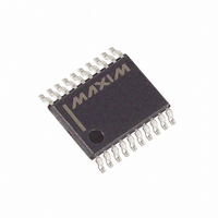
IC T-CHIP PHANTOM 3.3V 20-TSSOP
Manufacturer
Maxim Integrated Products
Type
Phantom Time Chipr
Datasheet
1.DS1315-5.pdf
(23 pages)
Specifications of DS1315E-33+
Time Format
HH:MM:SS:hh (12/24 hr)
Date Format
YY-MM-DD-dd
Interface
Parallel
Voltage - Supply
3 V ~ 3.6 V
Operating Temperature
0°C ~ 70°C
Mounting Type
Surface Mount
Package / Case
20-TSSOP
Lead Free Status / RoHS Status
Lead free / RoHS Compliant
Memory Size
-
DS1315 Phantom Time Chip
Operation
Communication with the Time Chip is established by pattern recognition of a serial bit stream of 64 bits
which must be matched by executing 64 consecutive write cycles containing the proper data on data in
(D). All accesses which occur prior to recognition of the 64-bit pattern are directed to memory via the
chip enable output pin (
).
CEO
After recognition is established, the next 64 read or write cycles either extract or update data in the Time
Chip and
remains high during this time, disabling the connected memory.
CEO
Data transfer to and from the timekeeping function is accomplished with a serial bit stream under control
of chip enable input (
), output enable (
), and write enable (
). Initially, a read cycle using the
CEI
OE
WE
and
control of the Time Chip starts the pattern recognition sequence by moving pointer to the
CEI
OE
first bit of the 64-bit comparison register. Next, 64 consecutive write cycles are executed using the
CEI
and
control of the Time Chip. These 64 write cycles are used only to gain access to the Time Chip.
WE
When the first write cycle is executed, it is compared to bit 1 of the 64-bit comparison register. If a match
is found, the pointer increments to the next location of the comparison register and awaits the next write
cycle. If a match is not found, the pointer does not advance and all subsequent write cycles are ignored. If
a read cycle occurs at any time during pattern recognition, the present sequence is aborted and the
comparison register pointer is reset. Pattern recognition continues for a total of 64 write cycles as
described above until all the bits in the comparison register have been matched. (This bit pattern is shown
in Figure 2). With a correct match for 64 bits, the Time Chip is enabled and data transfer to or from the
timekeeping registers may proceed. The next 64 cycles will cause the Time Chip to either receive data on
D, or transmit data on Q, depending on the level of
pin or the
pin. Cycles to other locations
OE
WE
outside the memory block can be interleaved with
cycles without interrupting the pattern recognition
CEI
sequence or data transfer sequence to the Time Chip.
A standard 32.768 kHz quartz crystal can be directly connected to the DS1315 via pins 1 and 2 (X1, X2).
The crystal selected for use should have a specified load capacitance (C
) of 6 pF. For more information
L
on crystal selection and crystal layout considerations, please consult Application Note 58, “Crystal
Considerations with Dallas Real Time Clocks.”
4 of 23


