DS12885SN+ Maxim Integrated Products, DS12885SN+ Datasheet - Page 10
DS12885SN+
Manufacturer Part Number
DS12885SN+
Description
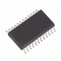
IC RTC W/RAM 128 BYTE IND 24SOIC
Manufacturer
Maxim Integrated Products
Type
Clock/Calendar/NVSRAMr
Datasheet
1.DS12885N.pdf
(22 pages)
Specifications of DS12885SN+
Memory Size
114B
Time Format
HH:MM:SS (12/24 hr)
Date Format
YY-MM-DD-dd
Interface
Parallel
Voltage - Supply
4.5 V ~ 5.5 V
Operating Temperature
-40°C ~ 85°C
Mounting Type
Surface Mount
Package / Case
24-SOIC (7.5mm Width)
Lead Free Status / RoHS Status
Lead free / RoHS Compliant


Real-Time Clocks
10
PDIP
SO,
19
20
21
23
24
____________________________________________________________________
DS12C887A)
(DS12887A/
EDIP
21
19
23
24
—
PIN
PLCC
25
23
24
27
28
TQFP
21
22
24
26
28
NAME
RCLR
V
SQW
V
IRQ
BAT
CC
Active-Low Interrupt Request Output. The IRQ pin is an active-low output of the
device that can be used as an interrupt input to a processor. The IRQ output
remains low as long as the status bit causing the interrupt is present and the
corresponding interrupt-enable bit is set. The processor program normally
reads the C register to clear the IRQ pin. The RESET pin also clears pending
interrupts. When no interrupt conditions are present, the IRQ level is in the high-
impedance state. Multiple interrupting devices can be connected to an IRQ
bus, provided that they are all open drain. The IRQ pin is an open-drain output
and requires an external pullup resistor to V
Connection for a Primary Battery. (DS12885 Only.) Battery voltage must be held
between the minimum and maximum limits for proper operation. If a backup
supply is not supplied, V
the V
prevent proper operation. UL recognized to ensure against reverse charging
when used with a lithium battery.
Active-Low RAM Clear. The RCLR pin is used to clear (set to logic 1) all the
general-purpose RAM, but does not affect the RAM associated with the RTC. To
clear the RAM, RCLR must be forced to an input logic 0 during battery-backup
mode when V
through a human interface (shorting to ground manually or by a switch) and not
to be driven with external buffers. This pin is internally pulled up. Do not use an
external pullup resistor on this pin.
Square-Wave Output. The SQW pin can output a signal from one of 13 taps
provided by the 15 internal divider stages of the RTC. The frequency of the
SQW pin can be changed by programming Register A, as shown in Table 1.
The SQW signal can be turned on and off using the SQWE bit in Register B. The
SQW signal is not available when V
DC Power Pin for Primary Power Supply. When V
limits, the device is fully accessible and data can be written and read. When
V
CC
is below V
BAT
pin. Diodes in series between the V
CC
PF
is not applied. The RCLR function is designed to be used
reads and writes are inhibited.
BAT
must be grounded. Connect the battery directly to
Pin Description (continued)
FUNCTION
CC
is less than V
CC
BAT
.
CC
pin and the battery may
PF
is applied within normal
.
Related parts for DS12885SN+
Image
Part Number
Description
Manufacturer
Datasheet
Request
R

Part Number:
Description:
IC RTC W/RAM 128 BYTE 24-DIP
Manufacturer:
Maxim Integrated Products
Datasheet:
Part Number:
Description:
IC RTC W/RAM 128 BYTE 24-DIP
Manufacturer:
Maxim Integrated Products
Datasheet:

Part Number:
Description:
Slide Switch,STRAIGHT,SPST,ON-OFF,Number Of Positions:12,PC TAIL Terminal,PCB Hole Count:24
Manufacturer:
APEM Components
Datasheet:

Part Number:
Description:
MAX7528KCWPMaxim Integrated Products [CMOS Dual 8-Bit Buffered Multiplying DACs]
Manufacturer:
Maxim Integrated Products
Datasheet:
Part Number:
Description:
Single +5V, fully integrated, 1.25Gbps laser diode driver.
Manufacturer:
Maxim Integrated Products
Datasheet:
Part Number:
Description:
Single +5V, fully integrated, 155Mbps laser diode driver.
Manufacturer:
Maxim Integrated Products
Datasheet:
Part Number:
Description:
VRD11/VRD10, K8 Rev F 2/3/4-Phase PWM Controllers with Integrated Dual MOSFET Drivers
Manufacturer:
Maxim Integrated Products
Datasheet:
Part Number:
Description:
Highly Integrated Level 2 SMBus Battery Chargers
Manufacturer:
Maxim Integrated Products
Datasheet:
Part Number:
Description:
Current Monitor and Accumulator with Integrated Sense Resistor; ; Temperature Range: -40°C to +85°C
Manufacturer:
Maxim Integrated Products
Part Number:
Description:
TSSOP 14/A°/RS-485 Transceivers with Integrated 100O/120O Termination Resis
Manufacturer:
Maxim Integrated Products
Part Number:
Description:
TSSOP 14/A°/RS-485 Transceivers with Integrated 100O/120O Termination Resis
Manufacturer:
Maxim Integrated Products
Part Number:
Description:
QFN 16/A°/AC-DC and DC-DC Peak-Current-Mode Converters with Integrated Step
Manufacturer:
Maxim Integrated Products
Part Number:
Description:
TDFN/A/65V, 1A, 600KHZ, SYNCHRONOUS STEP-DOWN REGULATOR WITH INTEGRATED SWI
Manufacturer:
Maxim Integrated Products
Part Number:
Description:
Integrated Temperature Controller f
Manufacturer:
Maxim Integrated Products
Part Number:
Description:
SOT23-6/I°/45MHz to 650MHz, Integrated IF VCOs with Differential Output
Manufacturer:
Maxim Integrated Products